Product Overview
The QM42391 is a WLAN 2.4 GHz dual FEM consisting of two
2.4 GHz multi-mode PA die with coupler and two LNA +
Switches.
The QM42391 is an 802.11ax front-end module in an ultra- small
footprint. The front-end module supports three TX bias modes:
high gain + high linearity, high gain + increased efficiency, low
gain + increased efficiency. The QM42391 also has BT high
power and BT low power modes. The architecture and interface
are optimized for next generation WLAN integration into handset
and tablet devices.
front-end module die kit
The
features chipset-specific
compatible control voltages to facilitate ease of use. With its low
power dissipation, the front-end Module die kit contributes to the
extended battery life of next generation WLAN solutions.
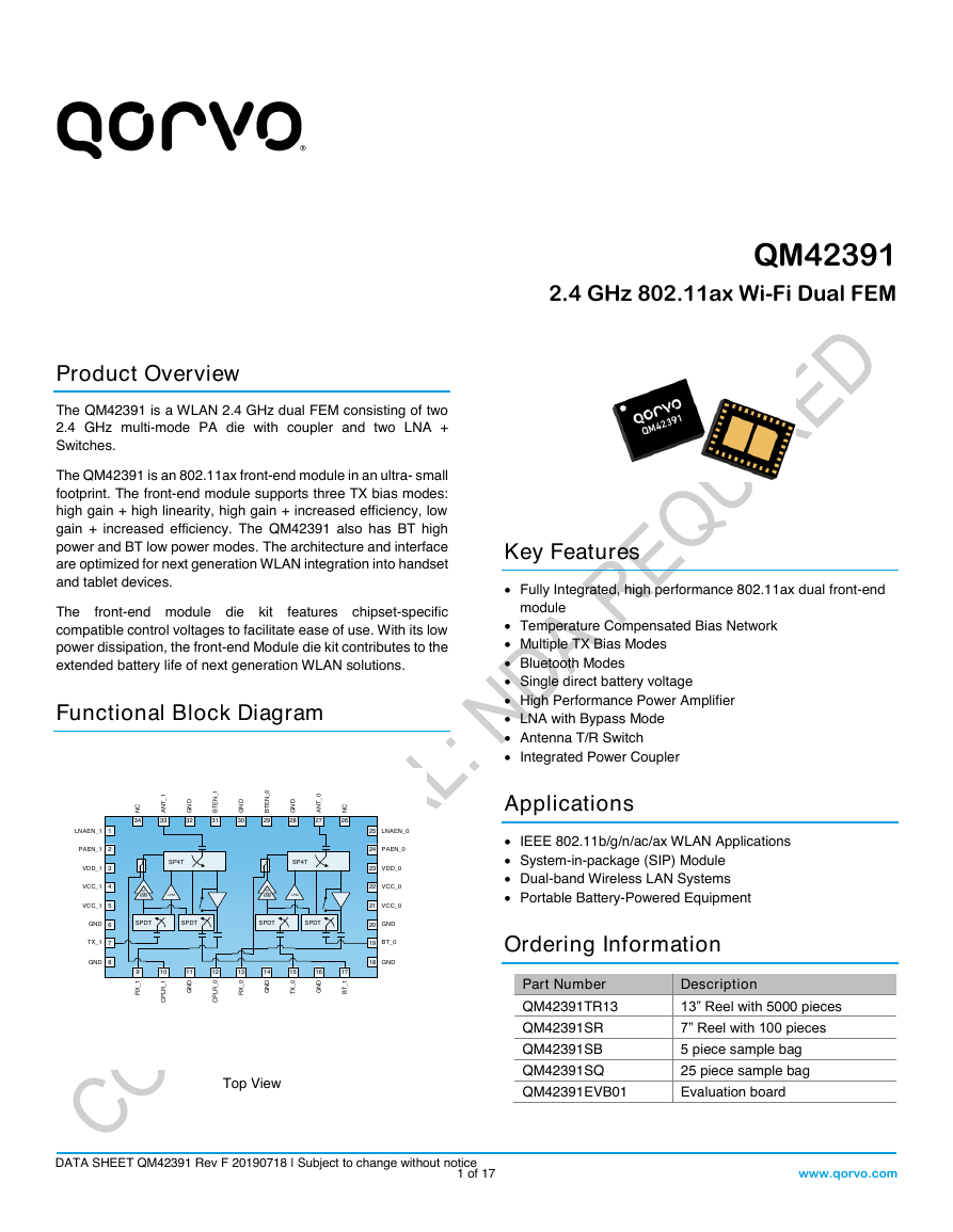
Functional Block Diagram
ADVANCED
ADVANCE
QM42391
D
2.4 GHz 802.11ax Wi-Fi Dual FEM
Key Features
• Fully Integrated, high performance 802.11ax dual front-end
module
• Temperature Compensated Bias Network
• Multiple TX Bias Modes
• Bluetooth Modes
• Single direct battery voltage
• High Performance Power Amplifier
• LNA with Bypass Mode
• Antenna T/R Switch
• Integrated Power Coupler
Applications
• IEEE 802.11b/g/n/ac/ax WLAN Applications
• System-in-package (SIP) Module
• Dual-band Wireless LAN Systems
• Portable Battery-Powered Equipment
Ordering Information
Part Number
Description
QM42391TR13
13” Reel with 5000 pieces
QM42391SR
QM42391SB
QM42391SQ
7” Reel with 100 pieces
5 piece sample bag
25 piece sample bag
QM42391EVB01
Evaluation board
Top View
DATA SHEET QM42391 Rev F 20190718 | Subject to change without notice
1 of 17
www.qorvo.com
SP4T BT HPMMPMLPM17BT_116GND15TX_014GND13RX_012CPLR_011GND10CPLR_19RX_126NC34NC33ANT_132GND31BTEN_130GND29BTEN_028GND27ANT_0 SPDT SPDT1LNAEN_12PAEN_13VDD_14VCC_15VCC_16GND7TX_18GND SP4T BT HPMMPMLPMSPDT SPDT18GND19BT_020GND21VCC_022VCC_023VDD_024PAEN_025LNAEN_0 �
QM42391
2.4 GHz 802.11ax Wi-Fi Dual FEM
Absolute Maximum Ratings
Parameter
Storage Temperature
Maximum Junction Temperature, Tj max
Device Voltage, VCC
Conditions
Rating
−40 to150 oC
150 oC
+6.0 V
RF Maximum Input Power (Tx Mode)
802.11n MCS0, 50Ω, VCC = 4.8 V, T = 25ºC
+12 dBm
RF Maximum Input Power (Rx/Bypass Mode)
802.11n MCS0, 50Ω, VCC = 4.8 V, T = 25ºC
+25 dBm
RF Maximum Input Power (BT High Power Mode) 802.11b, 1Mbps, 50Ω, VCC = 4.8 V, T = 25ºC +12 dBm
RF Maximum Input Power (BT Low Power Mode)
802.11b, 1Mbps, 50Ω, VCC = 4.8 V, T = 25ºC +25 dBm
RF Maximum Input Power (Tx Mode)
10:1 VSWR, VCC = 4.8 V, T = 25ºC
+5 dBm
Operation of this device outside the parameter ranges given above may cause permanent damage.
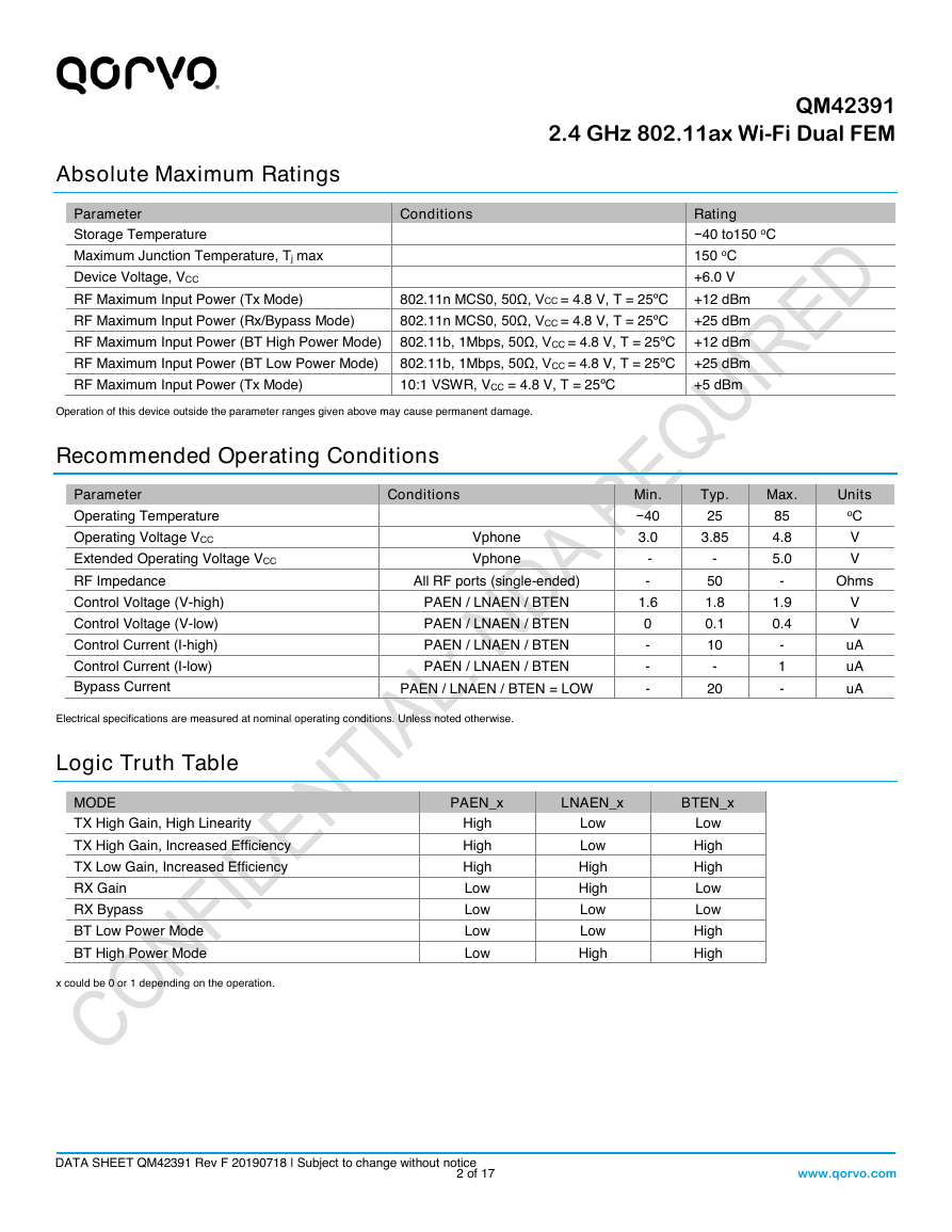
Recommended Operating Conditions
Parameter
Operating Temperature
Operating Voltage VCC
Extended Operating Voltage VCC
RF Impedance
Control Voltage (V-high)
Control Voltage (V-low)
Control Current (I-high)
Control Current (I-low)
Bypass Current
Conditions
Vphone
Vphone
All RF ports (single-ended)
PAEN / LNAEN / BTEN
PAEN / LNAEN / BTEN
PAEN / LNAEN / BTEN
PAEN / LNAEN / BTEN
PAEN / LNAEN / BTEN = LOW
Min.
−40
3.0
-
-
1.6
0
-
-
-
Typ.
25
3.85
-
50
1.8
0.1
10
-
20
Max.
Units
85
4.8
5.0
-
1.9
0.4
-
1
-
oC
V
V
Ohms
V
V
uA
uA
uA
Electrical specifications are measured at nominal operating conditions. Unless noted otherwise.
Logic Truth Table
MODE
TX High Gain, High Linearity
TX High Gain, Increased Efficiency
TX Low Gain, Increased Efficiency
RX Gain
RX Bypass
BT Low Power Mode
BT High Power Mode
x could be 0 or 1 depending on the operation.
PAEN_x
LNAEN_x
BTEN_x
High
High
High
Low
Low
Low
Low
Low
Low
High
High
Low
Low
High
Low
High
High
Low
Low
High
High
DATA SHEET QM42391 Rev F 20190718 | Subject to change without notice
2 of 17
www.qorvo.com
�
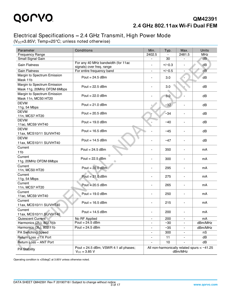
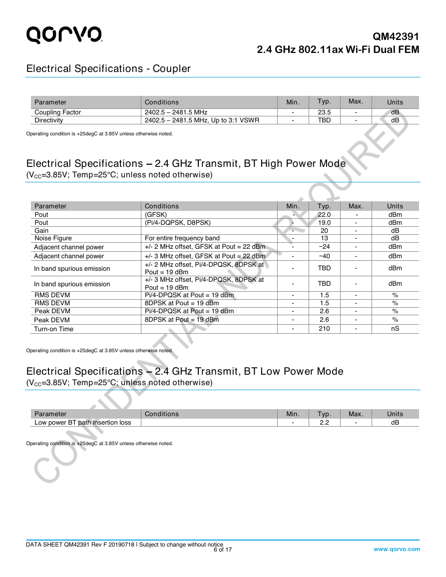
Electrical Specifications – 2.4 GHz Transmit, High Power Mode
(VCC=3.85V; Temp=25°C; unless noted otherwise)
QM42391
2.4 GHz 802.11ax Wi-Fi Dual FEM
Parameter
Frequency Range
Small Signal Gain
Gain Flatness
Gain Flatness
Margin to Spectrum Emission
Mask 11b
Margin to Spectrum Emission
Mask 11g, 20MHz OFDM 6Mbps
Margin to Spectrum Emission
Mask 11n, MCS0 HT20
DEVM
11g, 54 Mbps
DEVM
11n, MCS7 HT20
DEVM
11ac, MCS9 VHT40
DEVM
11ax, MCS10/11 SU/VHT40
DEVM
11ax, MCS10/11 SU/VHT40
Current
11b
Current
11g, 20MHz OFDM 6Mbps
Current
11n, MCS0 HT20
Current
11g, 54 Mbps
Current
11n, MCS7 HT20
Current
11ac, MCS9 VHT40
Current
11ax, MCS10/11 SU/VHT40
Current
11ax, MCS10/11 SU/VHT40
Quiescent Current
Harmonics (2f0), 802.11b
Harmonics (3f0), 802.11b
PA Switching Speed
Return Loss – TX Port
Return Loss – ANT Port
PA Stability
Conditions
For any 40 MHz bandwidth (for 11ac
signals) over freq. range
For entire frequency band
Pout = 24.5 dBm
Pout = 22.5 dBm
Pout = 22.0 dBm
Pout = 21.0 dBm
Pout = 20.5 dBm
Pout = 19.0 dBm
Pout = 16.5 dBm
Pout = 14.5 dBm
Pout = 24.5 dBm
Pout = 22.5 dBm
Pout = 22.0 dBm
Pout = 21.0 dBm
Pout = 20.5 dBm
Pout = 19.0 dBm
Pout = 16.5 dBm
Pout = 14.5 dBm
No RF Applied
Pout = 24.5 dBm
Pout = 24.5 dBm
Min.
2402.5
-
-
-
-
-
-
-
-
-
-
-
-
-
-
-
-
-
-
-
-
-
-
-
-
-
Typ.
-
30
+/−0.3
+/−0.5
3.0
3.0
3.0
−32
−34
−40
−45
−47
350
300
295
275
265
250
215
200
200
−30
−35
300
11
10
Max.
2481.5
-
-
-
-
-
-
-
-
-
-
-
-
-
-
-
-
-
-
-
-
-
-
-
-
-
Units
MHz
dB
dB
dB
dB
dB
dB
dB
dB
dB
dB
dB
mA
mA
mA
mA
mA
mA
mA
mA
mA
dBm/MHz
dBm/MHz
nS
dB
dB
Pout = 24.5 dBm; VSWR 4:1 all phases;
VCC = 3.85 V
All non-harmonically related spurs < −41.25
dBm/MHz
Operating condition is +25degC at 3.85V unless otherwise noted.
DATA SHEET QM42391 Rev F 20190718 | Subject to change without notice
3 of 17
www.qorvo.com
�
Electrical Specifications – 2.4 GHz Transmit, Mid Power Mode
(VCC=3.85V; Temp=25°C; unless noted otherwise)
QM42391
2.4 GHz 802.11ax Wi-Fi Dual FEM
Parameter
Frequency Range
Small Signal Gain
Gain Flatness
Gain Flatness
Margin to Spectrum Emission
Mask 11b
Margin to Spectrum Emission
Mask 11g, 20MHz OFDM 6Mbps
Margin to Spectrum Emission
Mask 11n, MCS0 HT20
DEVM
11g, 54 Mbps
DEVM
11n, MCS7 HT20
DEVM
11ac, MCS9 VHT40
DEVM
11ax, MCS10/11 SU/VHT40
DEVM
11ax, MCS10/11 SU/VHT40
Current
11b
Current
11g, 20MHz OFDM 6Mbps
Current
11n, MCS0 HT20
Current
11g, 54 Mbps
Current
11n, MCS7 HT20
Current
11ac, MCS9 VHT40
Current
11ax, MCS10/11 SU/VHT40
Current
11ax, MCS10/11 SU/VHT40
Quiescent Current
Harmonics (2f0), 802.11b
Harmonics (3f0), 802.11b
PA Switching Speed
Return Loss – TX Port
Return Loss – ANT Port
PA Stability
Conditions
For any 40 MHz bandwidth (for 11ac
signals) over freq. range
For entire frequency band
Pout = 21.5 dBm
Pout = 19.5 dBm
Pout = 19.0 dBm
Pout = 18.0 dBm
Pout = 18.0 dBm
Pout = 16.0 dBm
Pout = 13.5 dBm
Pout = 11.5 dBm
Pout = 21.5 dBm
Pout = 19.5 dBm
Pout = 19.0 dBm
Pout = 18.0 dBm
Pout = 18.0 dBm
Pout = 16.0 dBm
Pout = 13.5 dBm
Pout = 11.5 dBm
No RF Applied
Pout = 21.5 dBm
Pout = 21.5 dBm
Min.
2402.5
-
-
-
-
-
-
-
-
-
-
-
-
-
-
-
-
-
-
-
-
-
-
-
-
-
Typ.
-
27
+/−0.3
+/−0.5
3.0
3.0
3.0
−32
−34
−40
TBD
TBD
215
190
180
170
170
160
140
130
130
−50
−37
300
11
7
Max.
2481.5
-
-
-
-
-
-
-
-
-
-
-
-
-
-
-
-
-
-
-
-
-
-
-
-
-
Units
MHz
dB
dB
dB
dB
dB
dB
dB
dB
dB
dB
dB
mA
mA
mA
mA
mA
mA
mA
mA
mA
dBm/MHz
dBm/MHz
nS
dB
dB
Pout = 21.5 dBm; VSWR 4:1 all phases;
VCC = 3.85 V
All non-harmonically related spurs < −41.25
dBm/MHz
Operating condition is +25degC at 3.85V unless otherwise noted.
DATA SHEET QM42391 Rev F 20190718 | Subject to change without notice
4 of 17
www.qorvo.com
�
QM42391
2.4 GHz 802.11ax Wi-Fi Dual FEM
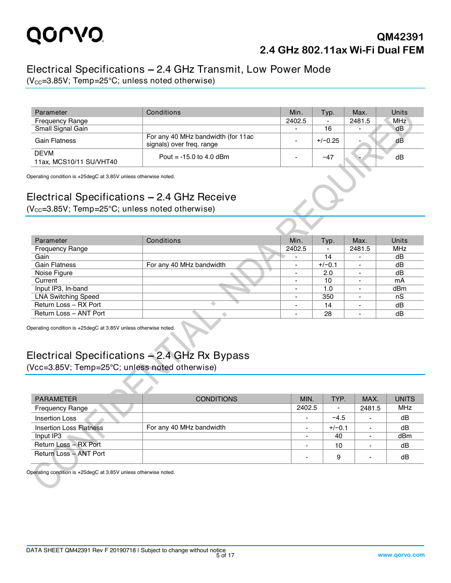
Electrical Specifications – 2.4 GHz Transmit, Low Power Mode
(VCC=3.85V; Temp=25°C; unless noted otherwise)
Parameter
Frequency Range
Small Signal Gain
Gain Flatness
DEVM
11ax, MCS10/11 SU/VHT40
Conditions
For any 40 MHz bandwidth (for 11ac
signals) over freq. range
Pout = -15.0 to 4.0 dBm
Min.
2402.5
-
-
-
Typ.
-
16
+/−0.25
−47
Max.
2481.5
-
-
-
Units
MHz
dB
dB
dB
Operating condition is +25degC at 3.85V unless otherwise noted.
Electrical Specifications – 2.4 GHz Receive
(VCC=3.85V; Temp=25°C; unless noted otherwise)
Parameter
Frequency Range
Gain
Gain Flatness
Noise Figure
Current
Input IP3, In-band
LNA Switching Speed
Return Loss – RX Port
Return Loss – ANT Port
Conditions
For any 40 MHz bandwidth
Min.
2402.5
-
-
-
-
-
-
-
-
Typ.
-
14
+/−0.1
2.0
10
1.0
350
14
28
Max.
2481.5
-
-
-
-
-
-
-
-
Units
MHz
dB
dB
dB
mA
dBm
nS
dB
dB
Operating condition is +25degC at 3.85V unless otherwise noted.
Electrical Specifications – 2.4 GHz Rx Bypass
(Vcc=3.85V; Temp=25°C; unless noted otherwise)
PARAMETER
Frequency Range
Insertion Loss
Insertion Loss Flatness
Input IP3
Return Loss – RX Port
Return Loss – ANT Port
CONDITIONS
For any 40 MHz bandwidth
MIN.
2402.5
-
-
-
-
-
TYP.
-
−4.5
+/−0.1
40
10
9
MAX.
2481.5
UNITS
MHz
-
-
-
-
-
dB
dB
dBm
dB
dB
Operating condition is +25degC at 3.85V unless otherwise noted.
DATA SHEET QM42391 Rev F 20190718 | Subject to change without notice
5 of 17
www.qorvo.com
�
QM42391
2.4 GHz 802.11ax Wi-Fi Dual FEM
Electrical Specifications - Coupler
Parameter
Coupling Factor
Directivity
Conditions
2402.5 – 2481.5 MHz
2402.5 – 2481.5 MHz, Up to 3:1 VSWR
Min.
-
-
Typ.
23.5
TBD
Max.
-
-
Units
dB
dB
Operating condition is +25degC at 3.85V unless otherwise noted.
Electrical Specifications – 2.4 GHz Transmit, BT High Power Mode
(VCC=3.85V; Temp=25°C; unless noted otherwise)
Parameter
Pout
Pout
Gain
Noise Figure
Adjacent channel power
Adjacent channel power
In band spurious emission
In band spurious emission
RMS DEVM
RMS DEVM
Peak DEVM
Peak DEVM
Turn-on Time
Conditions
(GFSK)
(Pi/4-DQPSK, D8PSK)
For entire frequency band
+/- 2 MHz offset, GFSK at Pout = 22 dBm
+/- 3 MHz offset, GFSK at Pout = 22 dBm
+/- 2 MHz offset, Pi/4-DPQSK, 8DPSK at
Pout = 19 dBm
+/- 3 MHz offset, Pi/4-DPQSK, 8DPSK at
Pout = 19 dBm
Pi/4-DPQSK at Pout = 19 dBm
8DPSK at Pout = 19 dBm
Pi/4-DPQSK at Pout = 19 dBm
8DPSK at Pout = 19 dBm
Min.
-
-
-
-
-
-
-
-
-
-
-
-
-
Typ.
22.0
19.0
20
13
−24
−40
TBD
TBD
1.5
1.5
2.6
2.6
210
Max.
-
-
-
-
-
-
-
-
-
-
-
-
-
Units
dBm
dBm
dB
dB
dBm
dBm
dBm
dBm
%
%
%
%
nS
Operating condition is +25degC at 3.85V unless otherwise noted.
Electrical Specifications – 2.4 GHz Transmit, BT Low Power Mode
(VCC=3.85V; Temp=25°C; unless noted otherwise)
Parameter
Low power BT path insertion loss
Conditions
Min.
-
Typ.
2.2
Max.
-
Units
dB
Operating condition is +25degC at 3.85V unless otherwise noted.
DATA SHEET QM42391 Rev F 20190718 | Subject to change without notice
6 of 17
www.qorvo.com
�
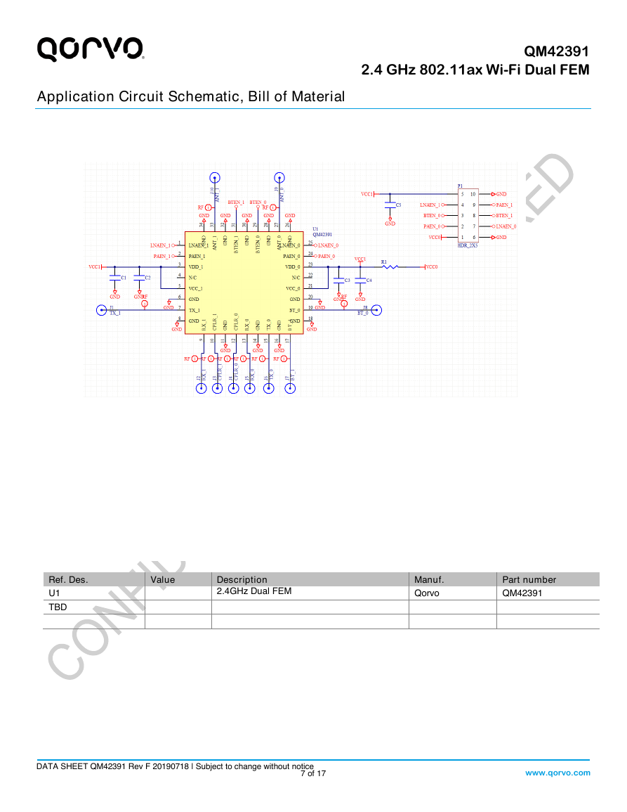
Application Circuit Schematic, Bill of Material
QM42391
2.4 GHz 802.11ax Wi-Fi Dual FEM
Ref. Des.
Value
U1
TBD
Description
2.4GHz Dual FEM
Manuf.
Qorvo
Part number
QM42391
DATA SHEET QM42391 Rev F 20190718 | Subject to change without notice
7 of 17
www.qorvo.com
�
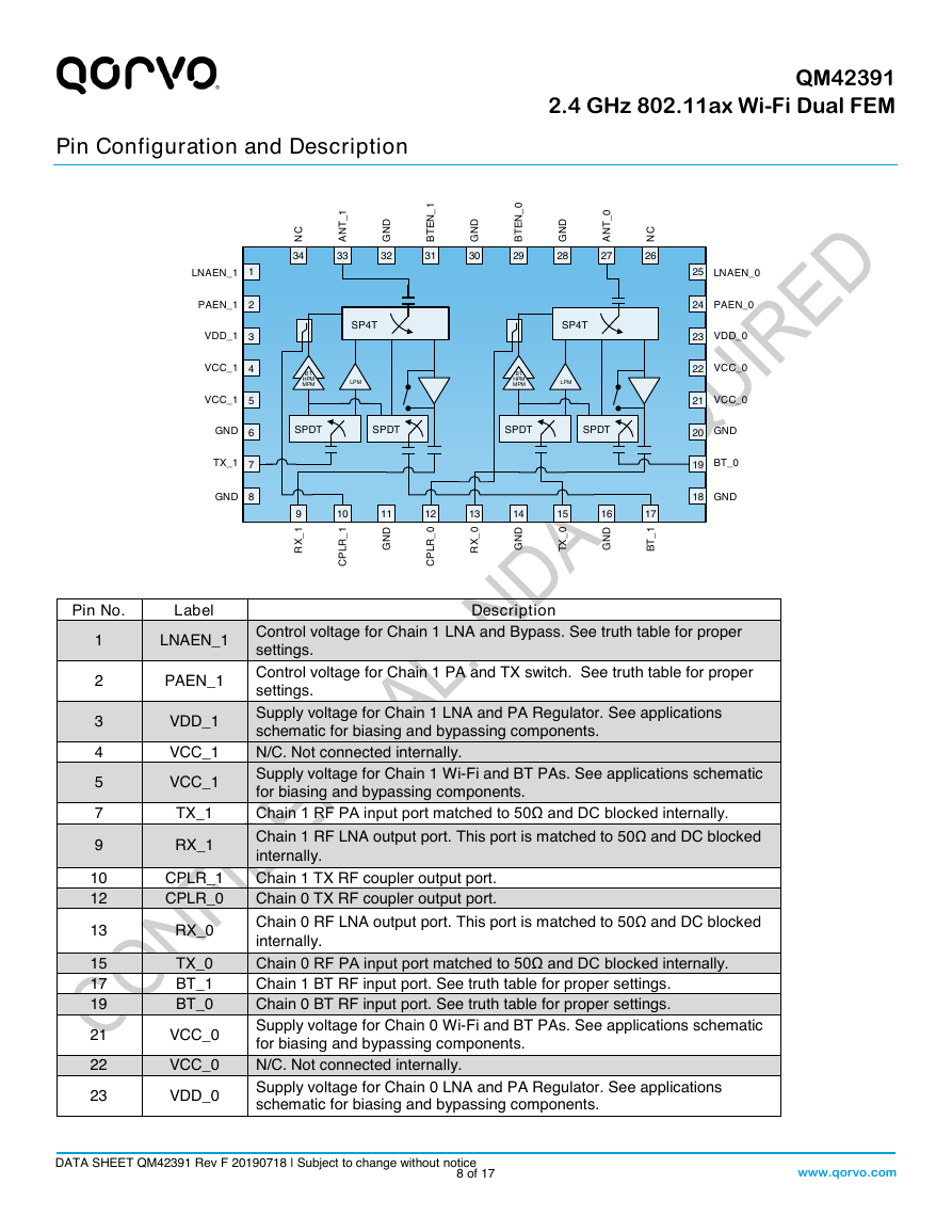
Pin Configuration and Description
QM42391
2.4 GHz 802.11ax Wi-Fi Dual FEM
Pin No.
Label
Description
1
2
3
4
5
7
9
10
12
13
15
17
19
21
22
23
LNAEN_1
Control voltage for Chain 1 LNA and Bypass. See truth table for proper
settings.
PAEN_1
Control voltage for Chain 1 PA and TX switch. See truth table for proper
settings.
VDD_1
VCC_1
VCC_1
TX_1
RX_1
CPLR_1
CPLR_0
RX_0
TX_0
BT_1
BT_0
VCC_0
VCC_0
VDD_0
Supply voltage for Chain 1 LNA and PA Regulator. See applications
schematic for biasing and bypassing components.
N/C. Not connected internally.
Supply voltage for Chain 1 Wi-Fi and BT PAs. See applications schematic
for biasing and bypassing components.
Chain 1 RF PA input port matched to 50Ω and DC blocked internally.
Chain 1 RF LNA output port. This port is matched to 50Ω and DC blocked
internally.
Chain 1 TX RF coupler output port.
Chain 0 TX RF coupler output port.
Chain 0 RF LNA output port. This port is matched to 50Ω and DC blocked
internally.
Chain 0 RF PA input port matched to 50Ω and DC blocked internally.
Chain 1 BT RF input port. See truth table for proper settings.
Chain 0 BT RF input port. See truth table for proper settings.
Supply voltage for Chain 0 Wi-Fi and BT PAs. See applications schematic
for biasing and bypassing components.
N/C. Not connected internally.
Supply voltage for Chain 0 LNA and PA Regulator. See applications
schematic for biasing and bypassing components.
DATA SHEET QM42391 Rev F 20190718 | Subject to change without notice
8 of 17
www.qorvo.com
SP4T BT HPMMPMLPM17BT_116GND15TX_014GND13RX_012CPLR_011GND10CPLR_19RX_126NC34NC33ANT_132GND31BTEN_130GND29BTEN_028GND27ANT_0 SPDT SPDT1LNAEN_12PAEN_13VDD_14VCC_15VCC_16GND7TX_18GND SP4T BT HPMMPMLPMSPDT SPDT18GND19BT_020GND21VCC_022VCC_023VDD_024PAEN_025LNAEN_0 �



 2023年江西萍乡中考道德与法治真题及答案.doc
 2012年重庆南川中考生物真题及答案.doc
 2013年江西师范大学地理学综合及文艺理论基础考研真题.doc
 2020年四川甘孜小升初语文真题及答案I卷.doc
 2020年注册岩土工程师专业基础考试真题及答案.doc
 2023-2024学年福建省厦门市九年级上学期数学月考试题及答案.doc
 2021-2022学年辽宁省沈阳市大东区九年级上学期语文期末试题及答案.doc
 2022-2023学年北京东城区初三第一学期物理期末试卷及答案.doc
 2018上半年江西教师资格初中地理学科知识与教学能力真题及答案.doc
 2012年河北国家公务员申论考试真题及答案-省级.doc
 2020-2021学年江苏省扬州市江都区邵樊片九年级上学期数学第一次质量检测试题及答案.doc
 2022下半年黑龙江教师资格证中学综合素质真题及答案.doc