MachXO2™ Family Data Sheet
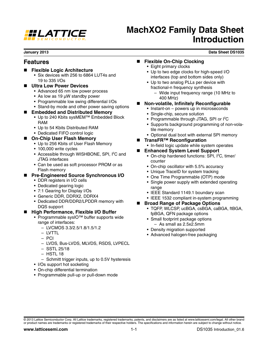
DS1035 Version 02.3, December 2013
�
MachXO2 Family Data Sheet
Introduction
Data Sheet DS1035
Flexible On-Chip Clocking
Eight primary clocks
Up to two edge clocks for high-speed I/O
interfaces (top and bottom sides only)
Up to two analog PLLs per device with
fractional-n frequency synthesis
– Wide input frequency range (10 MHz to
400 MHz)
Non-volatile, Infinitely Reconfigurable
Instant-on – powers up in microseconds
Single-chip, secure solution
Programmable through JTAG, SPI or I2C
Supports background programming of non-vola-
tile memory
Optional dual boot with external SPI memory
TransFR™ Reconfiguration
In-field logic update while system operates
Enhanced System Level Support
On-chip hardened functions: SPI, I2C, timer/
counter
On-chip oscillator with 5.5% accuracy
Unique TraceID for system tracking
One Time Programmable (OTP) mode
Single power supply with extended operating
range
IEEE Standard 1149.1 boundary scan
IEEE 1532 compliant in-system programming
Broad Range of Package Options
TQFP, WLCSP, ucBGA, csBGA, caBGA, ftBGA,
fpBGA, QFN package options
Small footprint package options
– As small as 2.5x2.5mm
Density migration supported
Advanced halogen-free packaging
January 2013
Features
Flexible Logic Architecture
• Six devices with 256 to 6864 LUT4s and
19 to 335 I/Os
Ultra Low Power Devices
Advanced 65 nm low power process
As low as 19 µW standby power
Programmable low swing differential I/Os
Stand-by mode and other power saving options
Embedded and Distributed Memory
Up to 240 Kbits sysMEM™ Embedded Block
RAM
Up to 54 Kbits Distributed RAM
Dedicated FIFO control logic
On-Chip User Flash Memory
Up to 256 Kbits of User Flash Memory
100,000 write cycles
Accessible through WISHBONE, SPI, I2C and
JTAG interfaces
Can be used as soft processor PROM or as
Flash memory
Pre-Engineered Source Synchronous I/O
DDR registers in I/O cells
Dedicated gearing logic
7:1 Gearing for Display I/Os
Generic DDR, DDRX2, DDRX4
Dedicated DDR/DDR2/LPDDR memory with
DQS support
High Performance, Flexible I/O Buffer
Programmable sysIO™ buffer supports wide
range of interfaces:
– LVCMOS 3.3/2.5/1.8/1.5/1.2
– LVTTL
– PCI
– LVDS, Bus-LVDS, MLVDS, RSDS, LVPECL
– SSTL 25/18
– HSTL 18
– Schmitt trigger inputs, up to 0.5V hysteresis
I/Os support hot socketing
On-chip differential termination
Programmable pull-up or pull-down mode
© 2013 Lattice Semiconductor Corp. All Lattice trademarks, registered trademarks, patents, and disclaimers are as listed at www.latticesemi.com/legal. All other brand
or product names are trademarks or registered trademarks of their respective holders. The specifications and information herein are subject to change without notice.
www.latticesemi.com
DS1035 Introduction_01.6
1-1
�
Introduction
MachXO2 Family Data Sheet
XO2-1200
1280
XO2-1200U1
1280
XO2-2000
2112
XO2-2000U1
2112
XO2-4000
4320
XO2-7000
6864
10
64
7
64
1
2
1
1
18
79
104
107
10
74
8
80
1
2
1
1
I/Os
206
16
74
8
80
1
2
1
1
79
104
111
206
206
16
92
10
96
2
2
1
1
278
34
92
10
96
2
2
1
1
104
114
150
206
206
274
278
54
240
26
256
2
2
1
1
114
206
206
278
334
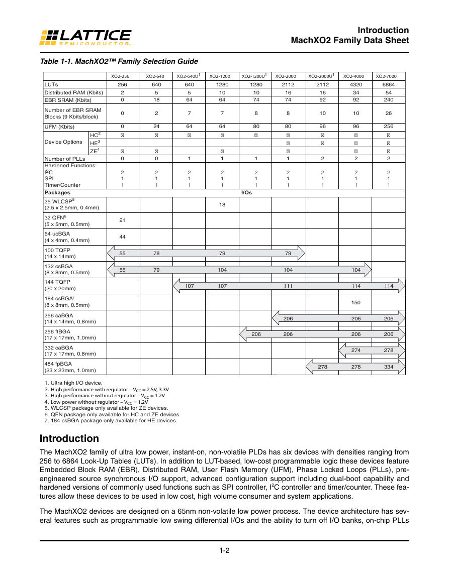
Table 1-1. MachXO2™ Family Selection Guide
XO2-256
256
XO2-640
640
2
0
0
0
0
2
1
1
21
44
55
55
5
18
2
24
0
2
1
1
78
79
XO2-640U1
640
5
64
7
64
1
2
1
1
107
LUTs
Distributed RAM (Kbits)
EBR SRAM (Kbits)
Number of EBR SRAM
Blocks (9 Kbits/block)
UFM (Kbits)
Device Options
HC2
HE3
ZE4
Number of PLLs
Hardened Functions:
I2C
SPI
Timer/Counter
Packages
25 WLCSP5
(2.5 x 2.5mm, 0.4mm)
32 QFN6
(5 x 5mm, 0.5mm)
64 ucBGA
(4 x 4mm, 0.4mm)
100 TQFP
(14 x 14mm)
132 csBGA
(8 x 8mm, 0.5mm)
144 TQFP
(20 x 20mm)
184 csBGA7
(8 x 8mm, 0.5mm)
256 caBGA
(14 x 14mm, 0.8mm)
256 ftBGA
(17 x 17mm, 1.0mm)
332 caBGA
(17 x 17mm, 0.8mm)
484 fpBGA
(23 x 23mm, 1.0mm)
1. Ultra high I/O device.
2. High performance with regulator – VCC = 2.5V, 3.3V
3. High performance without regulator – VCC = 1.2V
4. Low power without regulator – VCC = 1.2V
5. WLCSP package only available for ZE devices.
6. QFN package only available for HC and ZE devices.
7. 184 csBGA package only available for HE devices.
Introduction
The MachXO2 family of ultra low power, instant-on, non-volatile PLDs has six devices with densities ranging from
256 to 6864 Look-Up Tables (LUTs). In addition to LUT-based, low-cost programmable logic these devices feature
Embedded Block RAM (EBR), Distributed RAM, User Flash Memory (UFM), Phase Locked Loops (PLLs), pre-
engineered source synchronous I/O support, advanced configuration support including dual-boot capability and
hardened versions of commonly used functions such as SPI controller, I2C controller and timer/counter. These fea-
tures allow these devices to be used in low cost, high volume consumer and system applications.
The MachXO2 devices are designed on a 65nm non-volatile low power process. The device architecture has sev-
eral features such as programmable low swing differential I/Os and the ability to turn off I/O banks, on-chip PLLs
1-2
�
Introduction
MachXO2 Family Data Sheet
and oscillators dynamically. These features help manage static and dynamic power consumption resulting in low
static power for all members of the family.
The MachXO2 devices are available in two versions – ultra low power (ZE) and high performance (HC and HE)
devices. The ultra low power devices are offered in three speed grades -1, -2 and -3, with -3 being the fastest. Sim-
ilarly, the high-performance devices are offered in three speed grades: -4, -5 and -6, with -6 being the fastest. HC
devices have an internal linear voltage regulator which supports external VCC supply voltages of 3.3V or 2.5V. ZE
and HE devices only accept 1.2V as the external VCC supply voltage. With the exception of power supply voltage
all three types of devices (ZE, HC and HE) are functionally compatible and pin compatible with each other.
The MachXO2 PLDs are available in a broad range of advanced halogen-free packages ranging from the space
saving 2.5x2.5 mm WLCSP to the 23x23 mm fpBGA. MachXO2 devices support density migration within the same
package. Table 1-1 shows the LUT densities, package and I/O options, along with other key parameters.
The pre-engineered source synchronous logic implemented in the MachXO2 device family supports a broad range
of interface standards, including LPDDR, DDR, DDR2 and 7:1 gearing for display I/Os.
The MachXO2 devices offer enhanced I/O features such as drive strength control, slew rate control, PCI compati-
bility, bus-keeper latches, pull-up resistors, pull-down resistors, open drain outputs and hot socketing. Pull-up, pull-
down and bus-keeper features are controllable on a “per-pin” basis.
A user-programmable internal oscillator is included in MachXO2 devices. The clock output from this oscillator may
be divided by the timer/counter for use as clock input in functions such as LED control, key-board scanner and sim-
ilar state machines.
The MachXO2 devices also provide flexible, reliable and secure configuration from on-chip Flash memory. These
devices can also configure themselves from external SPI Flash or be configured by an external master through the
JTAG test access port or through the I2C port. Additionally, MachXO2 devices support dual-boot capability (using
external Flash memory) and remote field upgrade (TransFR) capability.
Lattice provides a variety of design tools that allow complex designs to be efficiently implemented using the
MachXO2 family of devices. Popular logic synthesis tools provide synthesis library support for MachXO2. Lattice
design tools use the synthesis tool output along with the user-specified preferences and constraints to place and
route the design in the MachXO2 device. These tools extract the timing from the routing and back-annotate it into
the design for timing verification.
Lattice provides many pre-engineered IP (Intellectual Property) LatticeCORE™ modules, including a number of
reference designs licensed free of charge, optimized for the MachXO2 PLD family. By using these configurable soft
core IP cores as standardized blocks, users are free to concentrate on the unique aspects of their design, increas-
ing their productivity.
1-3
�
MachXO2 Family Data Sheet
Architecture
December 2013
Data Sheet DS1035
Architecture Overview
The MachXO2 family architecture contains an array of logic blocks surrounded by Programmable I/O (PIO). The
larger logic density devices in this family have sysCLOCK™ PLLs and blocks of sysMEM Embedded Block RAM
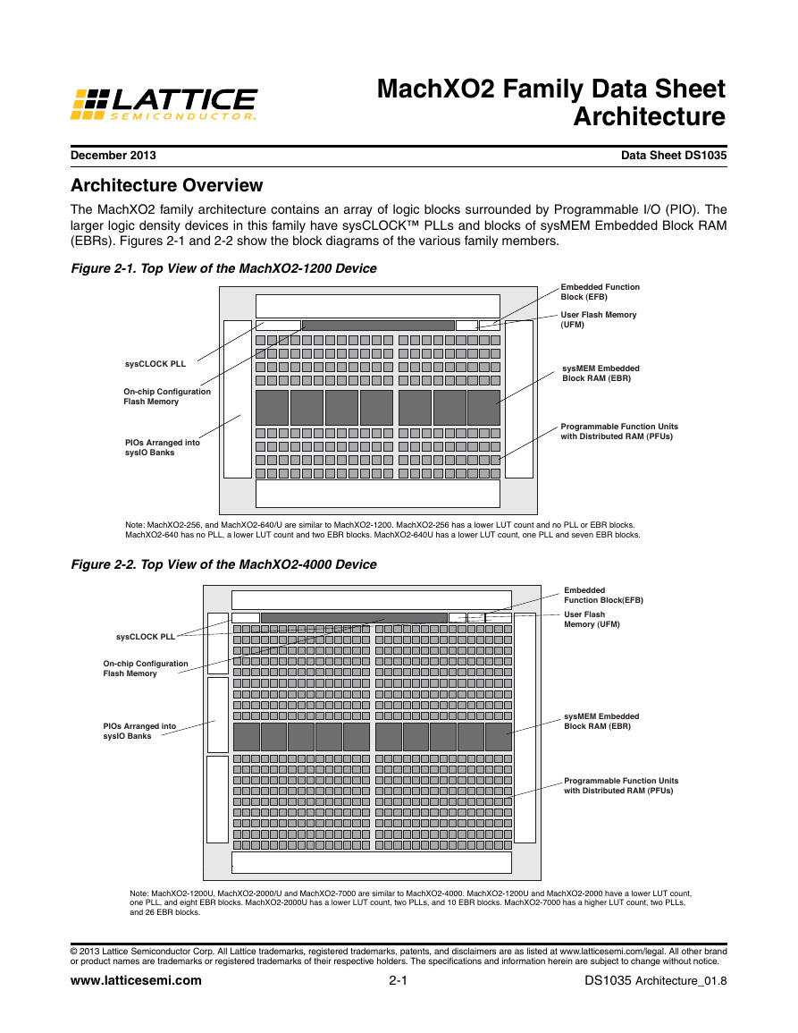
(EBRs). Figures 2-1 and 2-2 show the block diagrams of the various family members.
Figure 2-1. Top View of the MachXO2-1200 Device
sysCLOCK PLL
On-chip Configuration
Flash Memory
PIOs Arranged into
sysIO Banks
Embedded Function
Block (EFB)
User Flash Memory
(UFM)
sysMEM Embedded
Block RAM (EBR)
Programmable Function Units
with Distributed RAM (PFUs)
Note: MachXO2-256, and MachXO2-640/U are similar to MachXO2-1200. MachXO2-256 has a lower LUT count and no PLL or EBR blocks.
MachXO2-640 has no PLL, a lower LUT count and two EBR blocks. MachXO2-640U has a lower LUT count, one PLL and seven EBR blocks.
Figure 2-2. Top View of the MachXO2-4000 Device
sysCLOCK PLL
On-chip Configuration
Flash Memory
PIOs Arranged into
sysIO Banks
Embedded
Function Block(EFB)
User Flash
Memory (UFM)
sysMEM Embedded
Block RAM (EBR)
Programmable Function Units
with Distributed RAM (PFUs)
Note: MachXO2-1200U, MachXO2-2000/U and MachXO2-7000 are similar to MachXO2-4000. MachXO2-1200U and MachXO2-2000 have a lower LUT count,
one PLL, and eight EBR blocks. MachXO2-2000U has a lower LUT count, two PLLs, and 10 EBR blocks. MachXO2-7000 has a higher LUT count, two PLLs,
and 26 EBR blocks.
© 2013 Lattice Semiconductor Corp. All Lattice trademarks, registered trademarks, patents, and disclaimers are as listed at www.latticesemi.com/legal. All other brand
or product names are trademarks or registered trademarks of their respective holders. The specifications and information herein are subject to change without notice.
www.latticesemi.com
DS1035 Architecture_01.8
2-1
�
Architecture
MachXO2 Family Data Sheet
The logic blocks, Programmable Functional Unit (PFU) and sysMEM EBR blocks, are arranged in a two-dimen-
sional grid with rows and columns. Each row has either the logic blocks or the EBR blocks. The PIO cells are
located at the periphery of the device, arranged in banks. The PFU contains the building blocks for logic, arithmetic,
RAM, ROM, and register functions. The PIOs utilize a flexible I/O buffer referred to as a sysIO buffer that supports
operation with a variety of interface standards. The blocks are connected with many vertical and horizontal routing
channel resources. The place and route software tool automatically allocates these routing resources.
In the MachXO2 family, the number of sysIO banks varies by device. There are different types of I/O buffers on the
different banks. Refer to the details in later sections of this document. The sysMEM EBRs are large, dedicated fast
memory blocks; these blocks are found in MachXO2-640/U and larger devices. These blocks can be configured as
RAM, ROM or FIFO. FIFO support includes dedicated FIFO pointer and flag “hard” control logic to minimize LUT
usage.
The MachXO2 registers in PFU and sysI/O can be configured to be SET or RESET. After power up and device is
configured, the device enters into user mode with these registers SET/RESET according to the configuration set-
ting, allowing device entering to a known state for predictable system function.
The MachXO2 architecture also provides up to two sysCLOCK Phase Locked Loop (PLL) blocks on MachXO2-
640U, MachXO2-1200/U and larger devices. These blocks are located at the ends of the on-chip Flash block. The
PLLs have multiply, divide, and phase shifting capabilities that are used to manage the frequency and phase rela-
tionships of the clocks.
MachXO2 devices provide commonly used hardened functions such as SPI controller, I2C controller and timer/
counter. MachXO2-640/U and higher density devices also provide User Flash Memory (UFM). These hardened
functions and the UFM interface to the core logic and routing through a WISHBONE interface. The UFM can also
be accessed through the SPI, I2C and JTAG ports.
Every device in the family has a JTAG port that supports programming and configuration of the device as well as
access to the user logic. The MachXO2 devices are available for operation from 3.3V, 2.5V and 1.2V power sup-
plies, providing easy integration into the overall system.
PFU Blocks
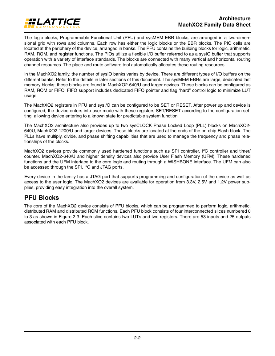
The core of the MachXO2 device consists of PFU blocks, which can be programmed to perform logic, arithmetic,
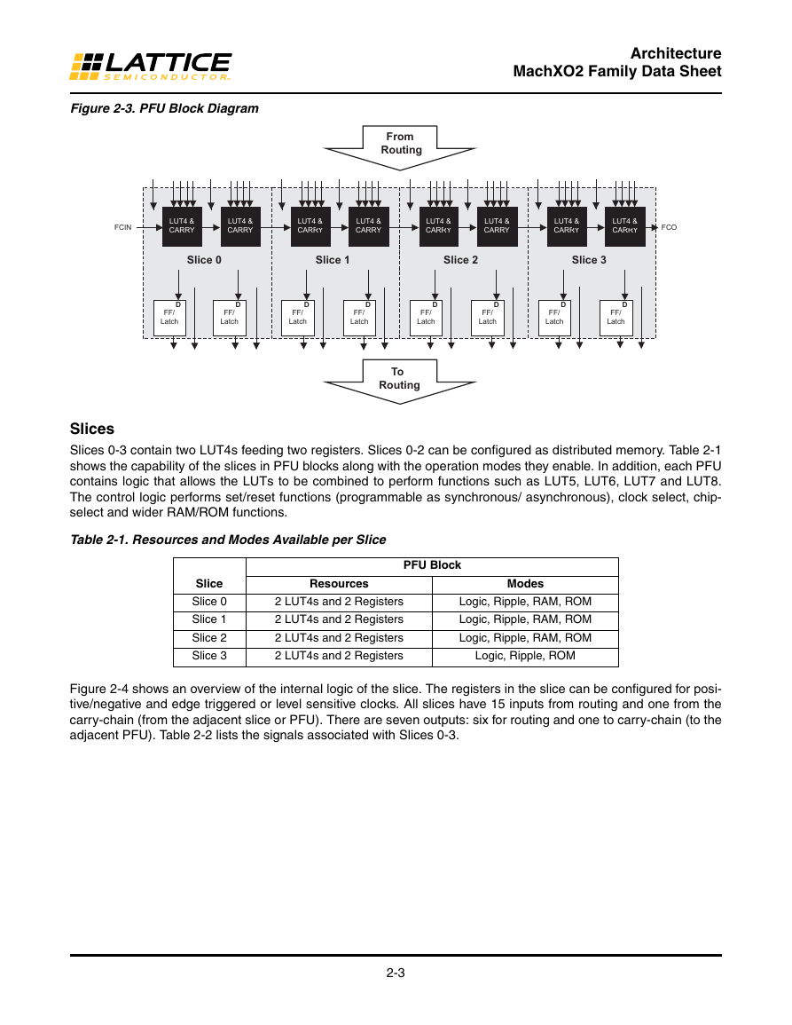
distributed RAM and distributed ROM functions. Each PFU block consists of four interconnected slices numbered 0
to 3 as shown in Figure 2-3. Each slice contains two LUTs and two registers. There are 53 inputs and 25 outputs
associated with each PFU block.
2-2
�
Figure 2-3. PFU Block Diagram
From
Routin g
Architecture
MachXO2 Family Data Sheet
FCIN
LUT4 &
CARRY
LUT4 &
CARRY
LUT4 &
CARRY
LUT4 &
CARRY
LUT4 &
CARRY
LUT4 &
CARRY
LUT4 &
CARRY
LUT4 &
CARRY
FCO
Slice 0
Slice 1
Slice 2
Slice 3
D
FF/
Latch
D
FF/
Latch
D
FF/
Latch
D
FF/
Latch
D
FF/
Latch
D
FF/
Latch
D
FF/
Latch
D
FF/
Latch
To
Routin g
Slices
Slices 0-3 contain two LUT4s feeding two registers. Slices 0-2 can be configured as distributed memory. Table 2-1
shows the capability of the slices in PFU blocks along with the operation modes they enable. In addition, each PFU
contains logic that allows the LUTs to be combined to perform functions such as LUT5, LUT6, LUT7 and LUT8.
The control logic performs set/reset functions (programmable as synchronous/ asynchronous), clock select, chip-
select and wider RAM/ROM functions.
Table 2-1. Resources and Modes Available per Slice
PFU Block
Slice
Slice 0
Slice 1
Slice 2
Slice 3
Resources
2 LUT4s and 2 Registers
2 LUT4s and 2 Registers
2 LUT4s and 2 Registers
2 LUT4s and 2 Registers
Modes
Logic, Ripple, RAM, ROM
Logic, Ripple, RAM, ROM
Logic, Ripple, RAM, ROM
Logic, Ripple, ROM
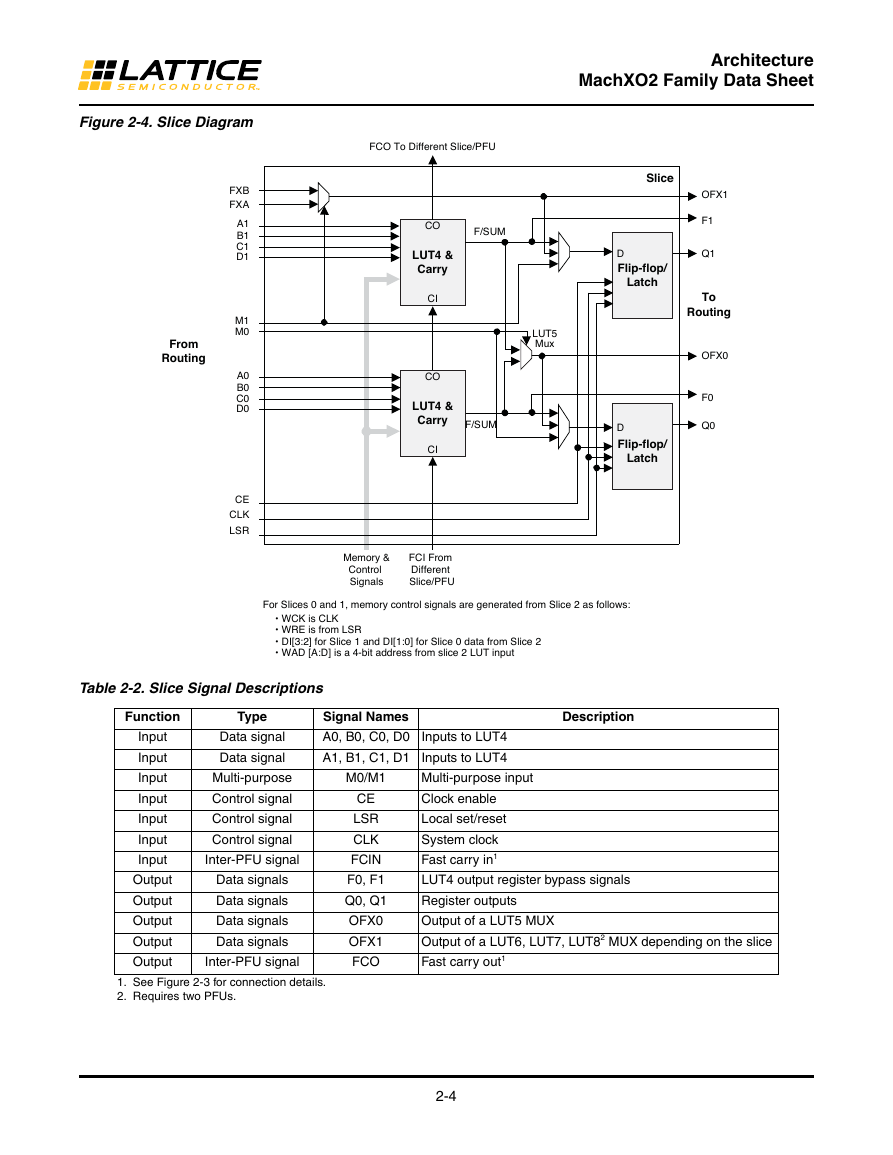
Figure 2-4 shows an overview of the internal logic of the slice. The registers in the slice can be configured for posi-
tive/negative and edge triggered or level sensitive clocks. All slices have 15 inputs from routing and one from the
carry-chain (from the adjacent slice or PFU). There are seven outputs: six for routing and one to carry-chain (to the
adjacent PFU). Table 2-2 lists the signals associated with Slices 0-3.
2-3
�
Architecture
MachXO2 Family Data Sheet
Slice
D
Flip-flop/
Latch
OFX1
F1
Q1
To
Routing
OFX0
F0
Q0
FCO To Different Slice/PFU
CO
F/SUM
LUT4 &
Carry
CI
CO
LUT4 &
Carry
CI
LUT5
Mux
F/SUM
D
Flip-flop/
Latch
Figure 2-4. Slice Diagram
From
Routing
FXB
FXA
A1
B1
C1
D1
M1
M0
A0
B0
C0
D0
CE
CLK
LSR
Memory &
Control
Signals
FCI From
Different
Slice/PFU
For Slices 0 and 1, memory control signals are generated from Slice 2 as follows:
• WCK is CLK
• WRE is from LSR
• DI[3:2] for Slice 1 and DI[1:0] for Slice 0 data from Slice 2
• WAD [A:D] is a 4-bit address from slice 2 LUT input
Table 2-2. Slice Signal Descriptions
Function
Type
Input
Input
Input
Input
Input
Input
Input
Output
Output
Output
Output
Output
Data signal
Data signal
Multi-purpose
Control signal
Control signal
Control signal
Inter-PFU signal
Data signals
Data signals
Data signals
Data signals
Inter-PFU signal
Signal Names
A0, B0, C0, D0 Inputs to LUT4
A1, B1, C1, D1 Inputs to LUT4
Description
M0/M1
CE
LSR
CLK
FCIN
F0, F1
Q0, Q1
OFX0
OFX1
FCO
Multi-purpose input
Clock enable
Local set/reset
System clock
Fast carry in1
LUT4 output register bypass signals
Register outputs
Output of a LUT5 MUX
Output of a LUT6, LUT7, LUT82 MUX depending on the slice
Fast carry out1
1. See Figure 2-3 for connection details.
2. Requires two PFUs.
2-4
�



 2023年江西萍乡中考道德与法治真题及答案.doc
 2012年重庆南川中考生物真题及答案.doc
 2013年江西师范大学地理学综合及文艺理论基础考研真题.doc
 2020年四川甘孜小升初语文真题及答案I卷.doc
 2020年注册岩土工程师专业基础考试真题及答案.doc
 2023-2024学年福建省厦门市九年级上学期数学月考试题及答案.doc
 2021-2022学年辽宁省沈阳市大东区九年级上学期语文期末试题及答案.doc
 2022-2023学年北京东城区初三第一学期物理期末试卷及答案.doc
 2018上半年江西教师资格初中地理学科知识与教学能力真题及答案.doc
 2012年河北国家公务员申论考试真题及答案-省级.doc
 2020-2021学年江苏省扬州市江都区邵樊片九年级上学期数学第一次质量检测试题及答案.doc
 2022下半年黑龙江教师资格证中学综合素质真题及答案.doc