logo资料库

micron_lpddr4.pdf

第1页 / 共286页
第2页 / 共286页
第3页 / 共286页
第4页 / 共286页
第5页 / 共286页
第6页 / 共286页
第7页 / 共286页
第8页 / 共286页
资料共286页,剩余部分请下载后查看
LPDDR4 SDRAM
Features
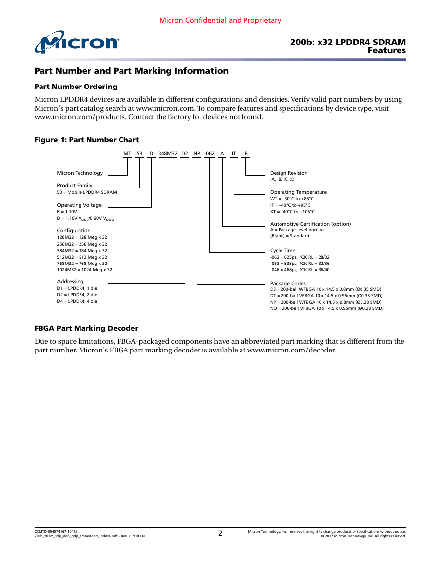
Part Number and Part Marking Information
Part Number Ordering
FBGA Part Marking Decoder
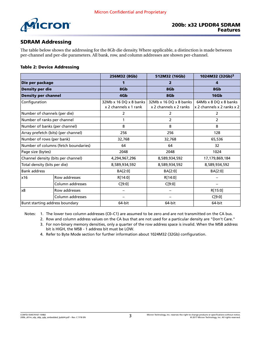
SDRAM Addressing
Important Notes and Warnings
General Description
General Notes
Package Block Diagrams
Ball Assignments and Descriptions
Package Dimensions
MR0, MR[6:3], MR8, MR13 Definition
IDD Parameters
Functional Description
Monolithic Device Addressing
Simplified Bus Interface State Diagram
Power-Up and Initialization
Voltage Ramp
Reset Initialization with Stable Power
Power-Off Sequence
Controlled Power-Off
Uncontrolled Power-Off
Mode Registers
Mode Register Assignments and Definitions
Commands and Timing
Truth Tables
ACTIVATE Command
Read and Write Access Modes
Preamble and Postamble
Burst READ Operation
Read Timing
tLZ(DQS), tLZ(DQ), tHZ(DQS), tHZ(DQ) Calculation
tLZ(DQS) and tHZ(DQS) Calculation for ATE (Automatic Test Equipment)
tLZ(DQ) and tHZ(DQ) Calculation for ATE (Automatic Test Equipment)
Burst WRITE Operation
Write Timing
tWPRE Calculation for ATE (Automatic Test Equipment)
tWPST Calculation for ATE (Automatic Test Equipment)
MASK WRITE Operation
Mask Write Timing Constraints for BL16
Data Mask and Data Bus Inversion (DBI [DC]) Function
Preamble and Postamble Behavior
Preamble, Postamble Behavior in READ-to-READ Operations
READ-to-READ Operations – Seamless
READ-to-READ Operations – Consecutive
WRITE-to-WRITE Operations – Seamless
WRITE-to-WRITE Operations – Consecutive
PRECHARGE Operation
Burst READ Operation Followed by Precharge
Burst WRITE Followed by Precharge
Auto Precharge
Burst READ With Auto Precharge
Burst WRITE With Auto Precharge
RAS Lock Function
Delay Time From WRITE-to-READ with Auto Precharge
REFRESH Command
Burst READ Operation Followed by Per Bank Refresh
Refresh Requirement
SELF REFRESH Operation
Self Refresh Entry and Exit
Power-Down Entry and Exit During Self Refresh
Command Input Timing After Power-Down Exit
Self Refresh Abort
MRR, MRW, MPC Commands During tXSR, tRFC
Power-Down Mode
Power-Down Entry and Exit
Input Clock Stop and Frequency Change
Clock Frequency Change – CKE LOW
Clock Stop – CKE LOW
Clock Frequency Change – CKE HIGH
Clock Stop – CKE HIGH
MODE REGISTER READ Operation
MRR After a READ and WRITE Command
MRR After Power-Down Exit
MODE REGISTER WRITE
Mode Register Write States
VREF Current Generator (VRCG)
VREF Training
VREF(CA) Training
VREF(DQ) Training
Command Bus Training
Command Bus Training Mode
Training Sequence for Single-Rank Systems
Training Sequence for Multiple-Rank Systems
Relation Between CA Input Pin and DQ Output Pin
Write Leveling
Mode Register Write-WR Leveling Mode
Write Leveling Procedure
Input Clock Frequency Stop and Change
MULTIPURPOSE Operation
Read DQ Calibration Training
Read DQ Calibration Training Procedure
Read DQ Calibration Training Example
MPC[READ DQ CALIBRATION] After Power-Down Exit
Write Training
Internal Interval Timer
DQS Interval Oscillator Matching Error
OSC Count Readout Time
Thermal Offset
Temperature Sensor
ZQ Calibration
ZQCAL Reset
Multichannel Considerations
ZQ External Resistor, Tolerance, and Capacitive Loading
Frequency Set Points
Frequency Set Point Update Timing
Pull-Up and Pull-Down Characteristics and Calibration
On-Die Termination for the Command/Address Bus
ODT Mode Register and ODT State Table
ODT Mode Register and ODT Characteristics
ODT for CA Update Time
DQ On-Die Termination
Output Driver and Termination Register Temperature and Voltage Sensitivity
ODT Mode Register
Asynchronous ODT
DQ ODT During Power-Down and Self Refresh Modes
ODT During Write Leveling Mode
Target Row Refresh Mode
TRR Mode Operation
Post-Package Repair
Failed Row Address Repair
Read Preamble Training
Electrical Specifications
Absolute Maximum Ratings
AC and DC Operating Conditions
AC and DC Input Measurement Levels
Input Levels for CKE
Input Levels for RESET_n
Differential Input Voltage for CK
Peak Voltage Calculation Method
Single-Ended Input Voltage for Clock
Differential Input Slew Rate Definition for Clock
Differential Input Cross-Point Voltage
Differential Input Voltage for DQS
Peak Voltage Calculation Method
Single-Ended Input Voltage for DQS
Differential Input Slew Rate Definition for DQS
Differential Input Cross-Point Voltage
Input Levels for ODT_CA
Output Slew Rate and Overshoot/Undershoot specifications
Single-Ended Output Slew Rate
Differential Output Slew Rate
Overshoot and Undershoot Specifications
Driver Output Timing Reference Load
LVSTL I/O System
Input/Output Capacitance
IDD Specification Parameters and Test Conditions
IDD Specifications
AC Timing
CA Rx Voltage and Timing
DQ Tx Voltage and Timing
DRAM Data Timing
DQ Rx Voltage and Timing
Clock Specification
tCK(abs), tCH(abs), and tCL(abs)
Clock Period Jitter
Clock Period Jitter Effects on Core Timing Parameters
Cycle Time Derating for Core Timing Parameters
Clock Cycle Derating for Core Timing Parameters
Clock Jitter Effects on Command/Address Timing Parameters
Clock Jitter Effects on READ Timing Parameters
Clock Jitter Effects on WRITE Timing Parameters
Byte Mode
Monolithic Device Addressing (Byte Mode)
Mode Register
Mode Register Assignments and Definitions
Command Bus Training
Training Mode 1
Training Sequence of Mode 1 for Single-Rank Systems
Training Sequence of Mode 1 for Multi-Rank Systems
Relation Between the CA Input Pin and the DQ Output Pin for Mode 1
Timing for CA Training Mode 1
Read DQ Calibration Training
Read DQ Calibration Training Procedure
Read DQ Calibration Training Example
AC Timing
Revision History
Rev. C – 7/18
Rev. B – 6/17
Rev. A – 3/17
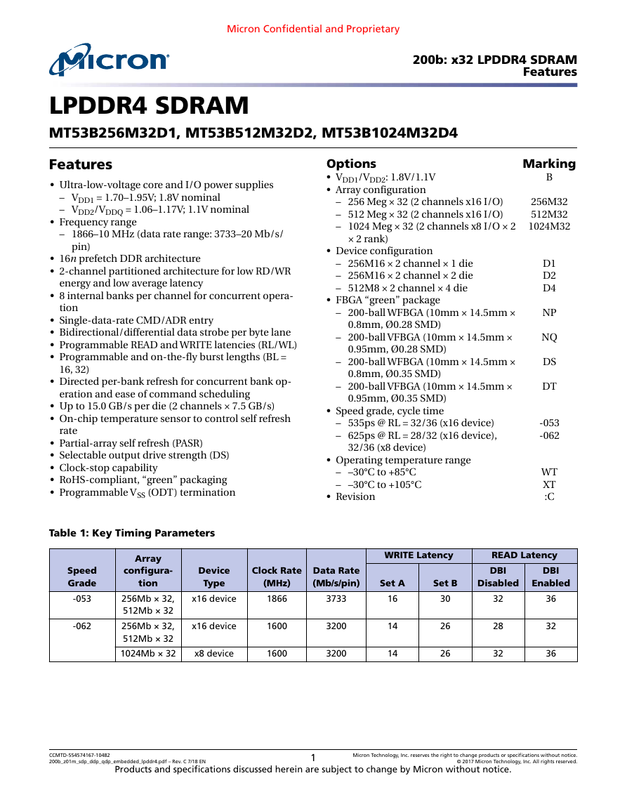
Micron Confidential and Proprietary 200b: x32 LPDDR4 SDRAM Features LPDDR4 SDRAM MT53B256M32D1, MT53B512M32D2, MT53B1024M32D4 Features • Ultra-low-voltage core and I/O power supplies – VDD1 = 1.70–1.95V; 1.8V nominal – VDD2/VDDQ = 1.06–1.17V; 1.1V nominal • Frequency range – 1866–10 MHz (data rate range: 3733–20 Mb/s/ pin) • 16n prefetch DDR architecture • 2-channel partitioned architecture for low RD/WR energy and low average latency • 8 internal banks per channel for concurrent opera- tion • Single-data-rate CMD/ADR entry • Bidirectional/differential data strobe per byte lane • Programmable READ and WRITE latencies (RL/WL) • Programmable and on-the-fly burst lengths (BL = 16, 32) • Directed per-bank refresh for concurrent bank op- eration and ease of command scheduling • Up to 15.0 GB/s per die (2 channels × 7.5 GB/s) • On-chip temperature sensor to control self refresh rate • Partial-array self refresh (PASR) • Selectable output drive strength (DS) • Clock-stop capability • RoHS-compliant, “green” packaging • Programmable VSS (ODT) termination Table 1: Key Timing Parameters Options • VDD1/VDD2: 1.8V/1.1V • Array configuration Marking B – 256 Meg × 32 (2 channels x16 I/O) – 512 Meg × 32 (2 channels x16 I/O) – 1024 Meg × 32 (2 channels x8 I/O × 2 256M32 512M32 1024M32 × 2 rank) • Device configuration – 256M16 × 2 channel × 1 die – 256M16 × 2 channel × 2 die – 512M8 × 2 channel × 4 die • FBGA “green” package – 200-ball WFBGA (10mm × 14.5mm × 0.8mm, Ø0.28 SMD) – 200-ball VFBGA (10mm × 14.5mm × 0.95mm, Ø0.28 SMD) – 200-ball WFBGA (10mm × 14.5mm × 0.8mm, Ø0.35 SMD) – 200-ball VFBGA (10mm × 14.5mm × 0.95mm, Ø0.35 SMD) • Speed grade, cycle time – 535ps @ RL = 32/36 (x16 device) – 625ps @ RL = 28/32 (x16 device), 32/36 (x8 device) • Operating temperature range – –30°C to +85°C – –30°C to +105°C • Revision D1 D2 D4 NP NQ DS DT -053 -062 WT XT :C Speed Grade -053 -062 Array configura- tion 256Mb × 32, 512Mb × 32 256Mb × 32, 512Mb × 32 1024Mb × 32 Device Type x16 device Clock Rate (MHz) 1866 x16 device 1600 x8 device 1600 Data Rate (Mb/s/pin) 3733 3200 3200 WRITE Latency READ Latency DBI DBI Set A Set B Disabled Enabled 16 14 14 30 26 26 32 28 32 36 32 36 CCMTD-554574167-10482 200b_z01m_sdp_ddp_qdp_embedded_lpddr4.pdf – Rev. C 7/18 EN Products and specifications discussed herein are subject to change by Micron without notice. 1 Micron Technology, Inc. reserves the right to change products or specifications without notice. © 2017 Micron Technology, Inc. All rights reserved.
Micron Confidential and Proprietary 200b: x32 LPDDR4 SDRAM Features Part Number and Part Marking Information Part Number Ordering Micron LPDDR4 devices are available in different configurations and densities. Verify valid part numbers by using Micron’s part catalog search at www.micron.com. To compare features and specifications by device type, visit www.micron.com/products. Contact the factory for devices not found. Figure 1: Part Number Chart MT 53 D 348M32 D2 NP -062 A IT :B Micron Technology Product Family 53 = Mobile LPDDR4 SDRAM Operating Voltage B = 1.10V D = 1.10V VDD2/0.60V VDDQ Configuration 128M32 = 128 Meg x 32 256M32 = 256 Meg x 32 384M32 = 384 Meg x 32 512M32 = 512 Meg x 32 768M32 = 768 Meg x 32 1024M32 = 1024 Meg x 32 Addressing D1 = LPDDR4, 1 die D2 = LPDDR4, 2 die D4 = LPDDR4, 4 die Design Revision :A, :B, :C, :D Operating Temperature WT = –30°C to +85°C IT = –40°C to +95°C XT = –40°C to +105°C Automotive Certification (option) A = Package-level burn-in (Blank) = Standard Cycle Time -062 = 625ps, tCK RL = 28/32 -053 = 535ps, tCK RL = 32/36 -046 = 468ps, tCK RL = 36/40 Package Codes DS = 200-ball WFBGA 10 x 14.5 x 0.8mm (Ø0.35 SMD) DT = 200-ball VFBGA 10 x 14.5 x 0.95mm (Ø0.35 SMD) NP = 200-ball WFBGA 10 x 14.5 x 0.8mm (Ø0.28 SMD) NQ = 200-ball VFBGA 10 x 14.5 x 0.95mm (Ø0.28 SMD) FBGA Part Marking Decoder Due to space limitations, FBGA-packaged components have an abbreviated part marking that is different from the part number. Micron’s FBGA part marking decoder is available at www.micron.com/decoder. CCMTD-554574167-10482 200b_z01m_sdp_ddp_qdp_embedded_lpddr4.pdf – Rev. C 7/18 EN 2 Micron Technology, Inc. reserves the right to change products or specifications without notice. © 2017 Micron Technology, Inc. All rights reserved.
Micron Confidential and Proprietary 200b: x32 LPDDR4 SDRAM Features SDRAM Addressing The table below shows the addressing for the 8Gb die density. Where applicable, a distinction is made between per-channel and per-die parameters. All bank, row, and column addresses are shown per-channel. Table 2: Device Addressing Die per package Density per die Density per channel Configuration Number of channels (per die) Number of ranks per channel Number of banks (per channel) Array prefetch (bits) (per channel) Number of rows (per bank) Number of columns (fetch boundaries) Page size (bytes) Channel density (bits per channel) Total density (bits per die) Bank address x16 Row addresses Column addresses Row addresses Column addresses x8 Burst starting address boundary 256M32 (8Gb) 512M32 (16Gb) 1024M32 (32Gb)3 1 8Gb 4Gb 2 8Gb 8Gb 4 8Gb 16Gb 32Mb x 16 DQ x 8 banks x 2 channels x 1 rank 32Mb x 16 DQ x 8 banks x 2 channels x 2 ranks 64Mb x 8 DQ x 8 banks x 2 channels x 2 ranks x 2 2 1 8 256 32,768 64 2048 2 2 8 256 32,768 64 2048 4,294,967,296 8,589,934,592 8,589,934,592 8,589,934,592 BA[2:0] R[14:0] C[9:0] – – 64-bit BA[2:0] R[14:0] C[9:0] – – 64-bit 2 2 8 128 65,536 32 1024 17,179,869,184 8,589,934,592 BA[2:0] – – R[15:0] C[9:0] 64-bit Notes: 1. The lower two column addresses (C0–C1) are assumed to be zero and are not transmitted on the CA bus. 2. Row and column address values on the CA bus that are not used for a particular density are "Don't Care." 3. For non-binary memory densities, only a quarter of the row address space is invalid. When the MSB address bit is HIGH, the MSB - 1 address bit must be LOW. 4. Refer to Byte Mode section for further information about 1024M32 (32Gb) configuration. CCMTD-554574167-10482 200b_z01m_sdp_ddp_qdp_embedded_lpddr4.pdf – Rev. C 7/18 EN 3 Micron Technology, Inc. reserves the right to change products or specifications without notice. © 2017 Micron Technology, Inc. All rights reserved.
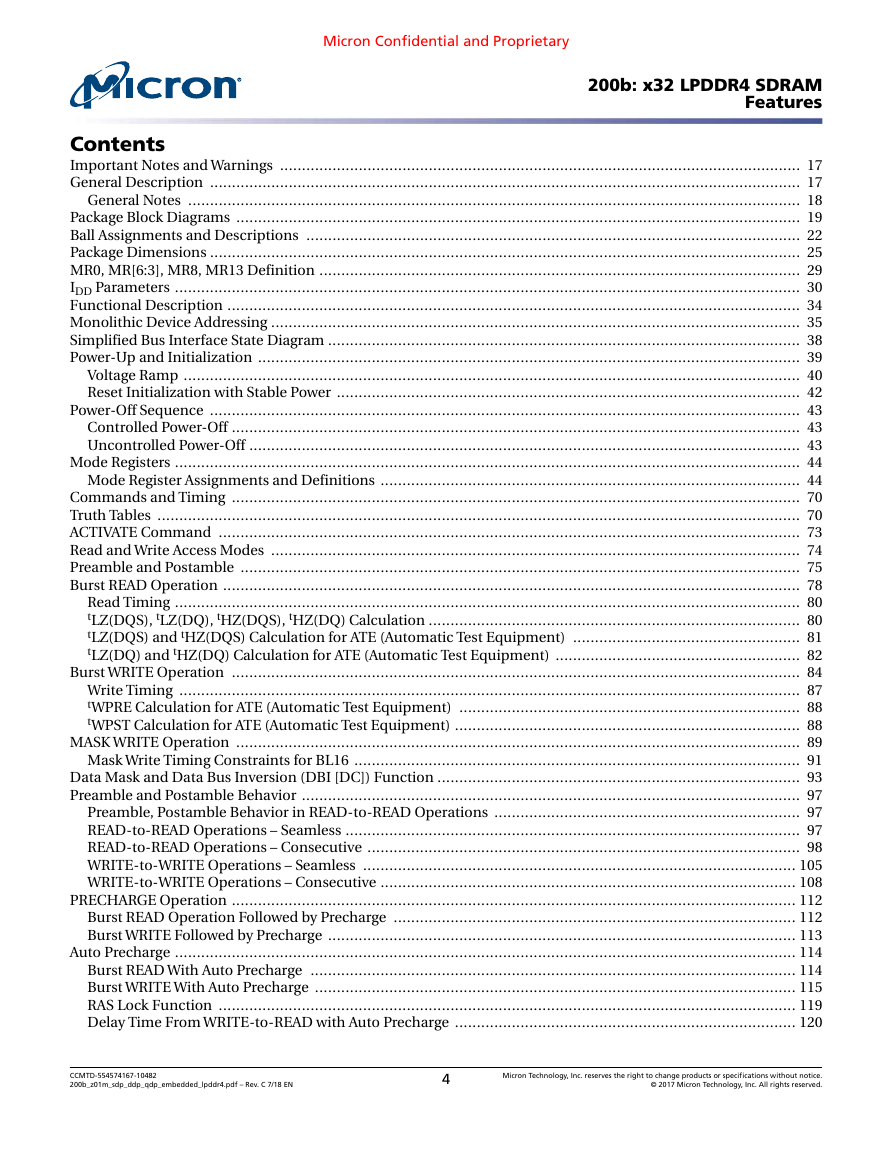
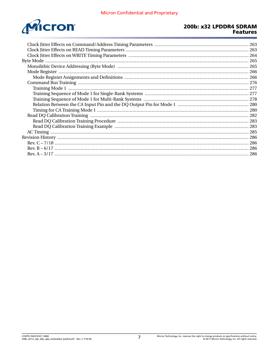
Micron Confidential and Proprietary 200b: x32 LPDDR4 SDRAM Features Contents Important Notes and Warnings ....................................................................................................................... 17 General Description ....................................................................................................................................... 17 General Notes ............................................................................................................................................ 18 Package Block Diagrams ................................................................................................................................. 19 Ball Assignments and Descriptions ................................................................................................................. 22 Package Dimensions ....................................................................................................................................... 25 MR0, MR[6:3], MR8, MR13 Definition .............................................................................................................. 29 IDD Parameters ............................................................................................................................................... 30 Functional Description ................................................................................................................................... 34 Monolithic Device Addressing ......................................................................................................................... 35 Simplified Bus Interface State Diagram ............................................................................................................ 38 Power-Up and Initialization ............................................................................................................................ 39 Voltage Ramp ............................................................................................................................................. 40 Reset Initialization with Stable Power .......................................................................................................... 42 Power-Off Sequence ....................................................................................................................................... 43 Controlled Power-Off .................................................................................................................................. 43 Uncontrolled Power-Off .............................................................................................................................. 43 Mode Registers ............................................................................................................................................... 44 Mode Register Assignments and Definitions ................................................................................................ 44 Commands and Timing .................................................................................................................................. 70 Truth Tables ................................................................................................................................................... 70 ACTIVATE Command ..................................................................................................................................... 73 Read and Write Access Modes ......................................................................................................................... 74 Preamble and Postamble ................................................................................................................................ 75 Burst READ Operation .................................................................................................................................... 78 Read Timing ............................................................................................................................................... 80 tLZ(DQS), tLZ(DQ), tHZ(DQS), tHZ(DQ) Calculation ..................................................................................... 80 tLZ(DQS) and tHZ(DQS) Calculation for ATE (Automatic Test Equipment) .................................................... 81 tLZ(DQ) and tHZ(DQ) Calculation for ATE (Automatic Test Equipment) ........................................................ 82 Burst WRITE Operation .................................................................................................................................. 84 Write Timing .............................................................................................................................................. 87 tWPRE Calculation for ATE (Automatic Test Equipment) .............................................................................. 88 tWPST Calculation for ATE (Automatic Test Equipment) ............................................................................... 88 MASK WRITE Operation ................................................................................................................................. 89 Mask Write Timing Constraints for BL16 ...................................................................................................... 91 Data Mask and Data Bus Inversion (DBI [DC]) Function ................................................................................... 93 Preamble and Postamble Behavior .................................................................................................................. 97 Preamble, Postamble Behavior in READ-to-READ Operations ...................................................................... 97 READ-to-READ Operations – Seamless ........................................................................................................ 97 READ-to-READ Operations – Consecutive ................................................................................................... 98 WRITE-to-WRITE Operations – Seamless ................................................................................................... 105 WRITE-to-WRITE Operations – Consecutive ............................................................................................... 108 PRECHARGE Operation ................................................................................................................................. 112 Burst READ Operation Followed by Precharge ............................................................................................ 112 Burst WRITE Followed by Precharge ........................................................................................................... 113 Auto Precharge .............................................................................................................................................. 114 Burst READ With Auto Precharge ............................................................................................................... 114 Burst WRITE With Auto Precharge .............................................................................................................. 115 RAS Lock Function .................................................................................................................................... 119 Delay Time From WRITE-to-READ with Auto Precharge .............................................................................. 120 CCMTD-554574167-10482 200b_z01m_sdp_ddp_qdp_embedded_lpddr4.pdf – Rev. C 7/18 EN 4 Micron Technology, Inc. reserves the right to change products or specifications without notice. © 2017 Micron Technology, Inc. All rights reserved.
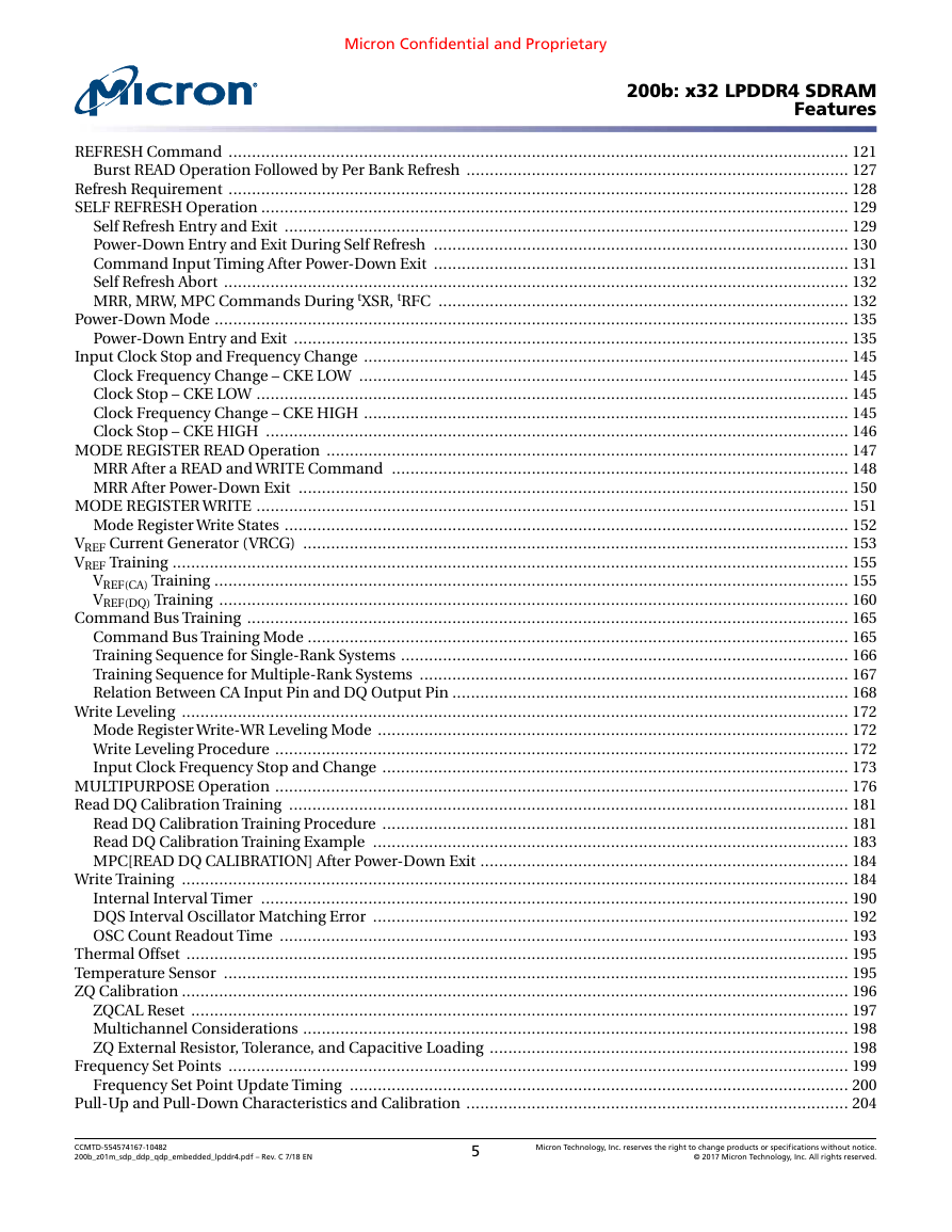
Micron Confidential and Proprietary 200b: x32 LPDDR4 SDRAM Features REFRESH Command ..................................................................................................................................... 121 Burst READ Operation Followed by Per Bank Refresh .................................................................................. 127 Refresh Requirement ..................................................................................................................................... 128 SELF REFRESH Operation .............................................................................................................................. 129 Self Refresh Entry and Exit ......................................................................................................................... 129 Power-Down Entry and Exit During Self Refresh ......................................................................................... 130 Command Input Timing After Power-Down Exit ......................................................................................... 131 Self Refresh Abort ...................................................................................................................................... 132 MRR, MRW, MPC Commands During tXSR, tRFC ........................................................................................ 132 Power-Down Mode ........................................................................................................................................ 135 Power-Down Entry and Exit ....................................................................................................................... 135 Input Clock Stop and Frequency Change ........................................................................................................ 145 Clock Frequency Change – CKE LOW ......................................................................................................... 145 Clock Stop – CKE LOW ............................................................................................................................... 145 Clock Frequency Change – CKE HIGH ........................................................................................................ 145 Clock Stop – CKE HIGH ............................................................................................................................. 146 MODE REGISTER READ Operation ................................................................................................................ 147 MRR After a READ and WRITE Command .................................................................................................. 148 MRR After Power-Down Exit ...................................................................................................................... 150 MODE REGISTER WRITE ............................................................................................................................... 151 Mode Register Write States ......................................................................................................................... 152 VREF Current Generator (VRCG) ..................................................................................................................... 153 VREF Training ................................................................................................................................................. 155 VREF(CA) Training ........................................................................................................................................ 155 VREF(DQ) Training ....................................................................................................................................... 160 Command Bus Training ................................................................................................................................. 165 Command Bus Training Mode .................................................................................................................... 165 Training Sequence for Single-Rank Systems ................................................................................................ 166 Training Sequence for Multiple-Rank Systems ............................................................................................ 167 Relation Between CA Input Pin and DQ Output Pin ..................................................................................... 168 Write Leveling ............................................................................................................................................... 172 Mode Register Write-WR Leveling Mode ..................................................................................................... 172 Write Leveling Procedure ........................................................................................................................... 172 Input Clock Frequency Stop and Change .................................................................................................... 173 MULTIPURPOSE Operation ........................................................................................................................... 176 Read DQ Calibration Training ........................................................................................................................ 181 Read DQ Calibration Training Procedure .................................................................................................... 181 Read DQ Calibration Training Example ...................................................................................................... 183 MPC[READ DQ CALIBRATION] After Power-Down Exit ............................................................................... 184 Write Training ............................................................................................................................................... 184 Internal Interval Timer .............................................................................................................................. 190 DQS Interval Oscillator Matching Error ...................................................................................................... 192 OSC Count Readout Time .......................................................................................................................... 193 Thermal Offset .............................................................................................................................................. 195 Temperature Sensor ...................................................................................................................................... 195 ZQ Calibration ............................................................................................................................................... 196 ZQCAL Reset ............................................................................................................................................. 197 Multichannel Considerations ..................................................................................................................... 198 ZQ External Resistor, Tolerance, and Capacitive Loading ............................................................................. 198 Frequency Set Points ..................................................................................................................................... 199 Frequency Set Point Update Timing ........................................................................................................... 200 Pull-Up and Pull-Down Characteristics and Calibration .................................................................................. 204 CCMTD-554574167-10482 200b_z01m_sdp_ddp_qdp_embedded_lpddr4.pdf – Rev. C 7/18 EN 5 Micron Technology, Inc. reserves the right to change products or specifications without notice. © 2017 Micron Technology, Inc. All rights reserved.
Micron Confidential and Proprietary 200b: x32 LPDDR4 SDRAM Features On-Die Termination for the Command/Address Bus ....................................................................................... 205 ODT Mode Register and ODT State Table .................................................................................................... 205 ODT Mode Register and ODT Characteristics ............................................................................................. 206 ODT for CA Update Time ........................................................................................................................... 208 DQ On-Die Termination ................................................................................................................................ 209 Output Driver and Termination Register Temperature and Voltage Sensitivity .............................................. 211 ODT Mode Register ................................................................................................................................... 212 Asynchronous ODT ................................................................................................................................... 212 DQ ODT During Power-Down and Self Refresh Modes ................................................................................ 214 ODT During Write Leveling Mode .............................................................................................................. 214 Target Row Refresh Mode ............................................................................................................................... 215 TRR Mode Operation ................................................................................................................................. 215 Post-Package Repair ...................................................................................................................................... 217 Failed Row Address Repair ......................................................................................................................... 217 Read Preamble Training ................................................................................................................................. 219 Electrical Specifications ................................................................................................................................. 220 Absolute Maximum Ratings ....................................................................................................................... 220 AC and DC Operating Conditions ................................................................................................................... 221 AC and DC Input Measurement Levels ........................................................................................................... 223 Input Levels for CKE .................................................................................................................................. 223 Input Levels for RESET_n ........................................................................................................................... 223 Differential Input Voltage for CK ................................................................................................................ 223 Peak Voltage Calculation Method ............................................................................................................... 224 Single-Ended Input Voltage for Clock ......................................................................................................... 225 Differential Input Slew Rate Definition for Clock ......................................................................................... 226 Differential Input Cross-Point Voltage ........................................................................................................ 227 Differential Input Voltage for DQS .............................................................................................................. 228 Peak Voltage Calculation Method ............................................................................................................... 228 Single-Ended Input Voltage for DQS ........................................................................................................... 229 Differential Input Slew Rate Definition for DQS .......................................................................................... 230 Differential Input Cross-Point Voltage ........................................................................................................ 231 Input Levels for ODT_CA ........................................................................................................................... 232 Output Slew Rate and Overshoot/Undershoot specifications ........................................................................... 232 Single-Ended Output Slew Rate .................................................................................................................. 232 Differential Output Slew Rate ..................................................................................................................... 233 Overshoot and Undershoot Specifications .................................................................................................. 234 Driver Output Timing Reference Load ............................................................................................................ 234 LVSTL I/O System .......................................................................................................................................... 235 Input/Output Capacitance ............................................................................................................................. 236 IDD Specification Parameters and Test Conditions ........................................................................................... 237 IDD Specifications ...................................................................................................................................... 243 AC Timing ..................................................................................................................................................... 245 CA Rx Voltage and Timing .............................................................................................................................. 254 DQ Tx Voltage and Timing ............................................................................................................................. 257 DRAM Data Timing ................................................................................................................................... 257 DQ Rx Voltage and Timing ............................................................................................................................. 258 Clock Specification ........................................................................................................................................ 261 tCK(abs), tCH(abs), and tCL(abs) ................................................................................................................ 262 Clock Period Jitter .......................................................................................................................................... 262 Clock Period Jitter Effects on Core Timing Parameters ................................................................................. 262 Cycle Time Derating for Core Timing Parameters ........................................................................................ 263 Clock Cycle Derating for Core Timing Parameters ....................................................................................... 263 CCMTD-554574167-10482 200b_z01m_sdp_ddp_qdp_embedded_lpddr4.pdf – Rev. C 7/18 EN 6 Micron Technology, Inc. reserves the right to change products or specifications without notice. © 2017 Micron Technology, Inc. All rights reserved.
Micron Confidential and Proprietary 200b: x32 LPDDR4 SDRAM Features Clock Jitter Effects on Command/Address Timing Parameters ..................................................................... 263 Clock Jitter Effects on READ Timing Parameters .......................................................................................... 263 Clock Jitter Effects on WRITE Timing Parameters ........................................................................................ 264 Byte Mode ..................................................................................................................................................... 265 Monolithic Device Addressing (Byte Mode) ................................................................................................ 265 Mode Register ........................................................................................................................................... 266 Mode Register Assignments and Definitions ........................................................................................... 266 Command Bus Training ............................................................................................................................. 276 Training Mode 1 .................................................................................................................................... 277 Training Sequence of Mode 1 for Single-Rank Systems ............................................................................ 277 Training Sequence of Mode 1 for Multi-Rank Systems ............................................................................. 278 Relation Between the CA Input Pin and the DQ Output Pin for Mode 1 .................................................... 280 Timing for CA Training Mode 1 ............................................................................................................... 280 Read DQ Calibration Training .................................................................................................................... 282 Read DQ Calibration Training Procedure ................................................................................................ 283 Read DQ Calibration Training Example .................................................................................................. 283 AC Timing ................................................................................................................................................. 285 Revision History ............................................................................................................................................ 286 Rev. C – 7/18 .............................................................................................................................................. 286 Rev. B – 6/17 .............................................................................................................................................. 286 Rev. A – 3/17 .............................................................................................................................................. 286 CCMTD-554574167-10482 200b_z01m_sdp_ddp_qdp_embedded_lpddr4.pdf – Rev. C 7/18 EN 7 Micron Technology, Inc. reserves the right to change products or specifications without notice. © 2017 Micron Technology, Inc. All rights reserved.
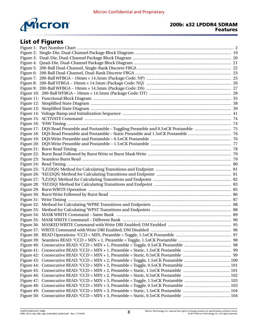
Micron Confidential and Proprietary 200b: x32 LPDDR4 SDRAM Features List of Figures Figure 1: Part Number Chart ............................................................................................................................ 2 Figure 2: Single-Die, Dual-Channel Package Block Diagram ............................................................................ 19 Figure 3: Dual-Die, Dual-Channel Package Block Diagram .............................................................................. 20 Figure 4: Quad-Die, Dual-Channel Package Block Diagram ............................................................................. 21 Figure 5: 200-Ball Dual-Channel, Single-Rank Discrete FBGA .......................................................................... 22 Figure 6: 200-Ball Dual-Channel, Dual-Rank Discrete FBGA ............................................................................ 23 Figure 7: 200-Ball WFBGA – 10mm × 14.5mm (Package Code: NP) ................................................................... 25 Figure 8: 200-Ball VFBGA – 10mm × 14.5mm (Package Code: NQ) ................................................................... 26 Figure 9: 200-Ball WFBGA – 10mm × 14.5mm (Package Code: DS) ................................................................... 27 Figure 10: 200-Ball WFBGA – 10mm × 14.5mm (Package Code: DT) ................................................................. 28 Figure 11: Functional Block Diagram ............................................................................................................. 35 Figure 12: Simplified State Diagram ............................................................................................................... 38 Figure 13: Simplified State Diagram ............................................................................................................... 39 Figure 14: Voltage Ramp and Initialization Sequence ...................................................................................... 41 Figure 15: ACTIVATE Command .................................................................................................................... 74 Figure 16: tFAW Timing .................................................................................................................................. 74 Figure 17: DQS Read Preamble and Postamble – Toggling Preamble and 0.5nCK Postamble ............................. 75 Figure 18: DQS Read Preamble and Postamble – Static Preamble and 1.5nCK Postamble .................................. 76 Figure 19: DQS Write Preamble and Postamble – 0.5nCK Postamble ................................................................ 76 Figure 20: DQS Write Preamble and Postamble – 1.5nCK Postamble ................................................................ 77 Figure 21: Burst Read Timing ......................................................................................................................... 78 Figure 22: Burst Read Followed by Burst Write or Burst Mask Write .................................................................. 79 Figure 23: Seamless Burst Read ...................................................................................................................... 79 Figure 24: Read Timing .................................................................................................................................. 80 Figure 25: tLZ(DQS) Method for Calculating Transitions and Endpoint ............................................................ 81 Figure 26: tHZ(DQS) Method for Calculating Transitions and Endpoint ........................................................... 81 Figure 27: tLZ(DQ) Method for Calculating Transitions and Endpoint .............................................................. 82 Figure 28: tHZ(DQ) Method for Calculating Transitions and Endpoint ............................................................. 83 Figure 29: Burst WRITE Operation ................................................................................................................. 85 Figure 30: Burst Write Followed by Burst Read ................................................................................................ 86 Figure 31: Write Timing ................................................................................................................................. 87 Figure 32: Method for Calculating tWPRE Transitions and Endpoints ............................................................... 88 Figure 33: Method for Calculating tWPST Transitions and Endpoints ............................................................... 88 Figure 34: MASK WRITE Command – Same Bank ........................................................................................... 89 Figure 35: MASK WRITE Command – Different Bank ...................................................................................... 90 Figure 36: MASKED WRITE Command with Write DBI Enabled; DM Enabled .................................................. 95 Figure 37: WRITE Command with Write DBI Enabled; DM Disabled ................................................................ 96 Figure 38: READ Operations: tCCD = MIN, Preamble = Toggle, 1.5nCK Postamble ............................................ 97 Figure 39: Seamless READ: tCCD = MIN + 1, Preamble = Toggle, 1.5nCK Postamble .......................................... 98 Figure 40: Consecutive READ: tCCD = MIN + 1, Preamble = Toggle, 0.5nCK Postamble ..................................... 98 Figure 41: Consecutive READ: tCCD = MIN + 1, Preamble = Static, 1.5nCK Postamble ...................................... 99 Figure 42: Consecutive READ: tCCD = MIN + 1, Preamble = Static, 0.5nCK Postamble ...................................... 99 Figure 43: Consecutive READ: tCCD = MIN + 2, Preamble = Toggle, 1.5nCK Postamble .................................... 100 Figure 44: Consecutive READ: tCCD = MIN + 2, Preamble = Toggle, 0.5nCK Postamble .................................... 101 Figure 45: Consecutive READ: tCCD = MIN + 2, Preamble = Static, 1.5nCK Postamble ..................................... 101 Figure 46: Consecutive READ: tCCD = MIN + 2, Preamble = Static, 0.5nCK Postamble ..................................... 102 Figure 47: Consecutive READ: tCCD = MIN + 3, Preamble = Toggle, 1.5nCK Postamble .................................... 103 Figure 48: Consecutive READ: tCCD = MIN + 3, Preamble = Toggle, 0.5nCK Postamble .................................... 103 Figure 49: Consecutive READ: tCCD = MIN + 3, Preamble = Static, 1.5nCK Postamble ..................................... 104 Figure 50: Consecutive READ: tCCD = MIN + 3, Preamble = Static, 0.5nCK Postamble ..................................... 104 CCMTD-554574167-10482 200b_z01m_sdp_ddp_qdp_embedded_lpddr4.pdf – Rev. C 7/18 EN 8 Micron Technology, Inc. reserves the right to change products or specifications without notice. © 2017 Micron Technology, Inc. All rights reserved.
分享到:
收藏