logo资料库

镁光8+8eMCP芯片规格书.pdf

第1页 / 共176页
第2页 / 共176页
第3页 / 共176页
第4页 / 共176页
第5页 / 共176页
第6页 / 共176页
第7页 / 共176页
第8页 / 共176页
资料共176页,剩余部分请下载后查看
MLC e·MMC™ and Mobile LPDDR3
221-Ball MCP
Features
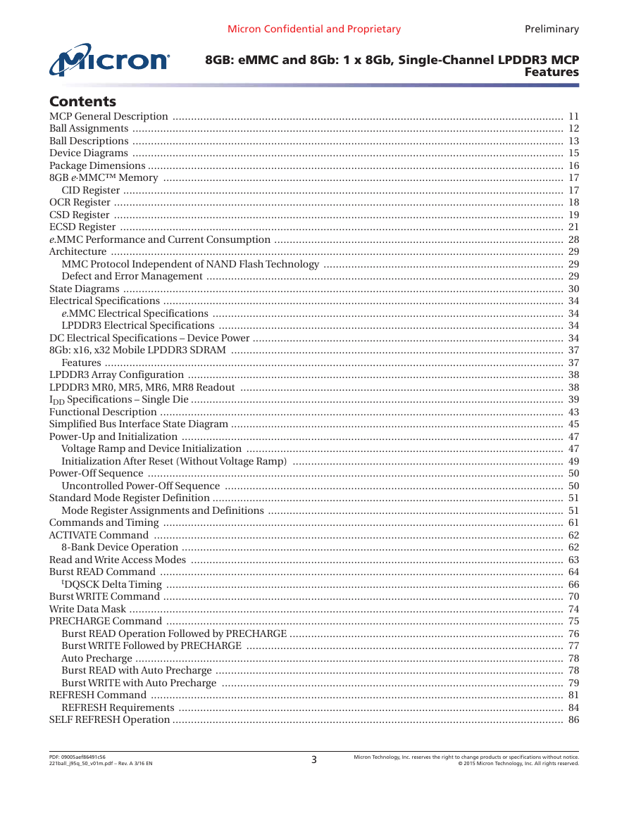
Part Numbering Information
Device Marking
MCP General Description
Ball Assignments
Ball Descriptions
Device Diagrams
Package Dimensions
8GB e·MMC™ Memory
CID Register
OCR Register
CSD Register
ECSD Register
e.MMC Performance and Current Consumption
Architecture
MMC Protocol Independent of NAND Flash Technology
Defect and Error Management
State Diagrams
Electrical Specifications
e.MMC Electrical Specifications
LPDDR3 Electrical Specifications
DC Electrical Specifications – Device Power
8Gb: x16, x32 Mobile LPDDR3 SDRAM
Features
LPDDR3 Array Configuration
LPDDR3 MR0, MR5, MR6, MR8 Readout
IDD Specifications – Single Die
Functional Description
Simplified Bus Interface State Diagram
Power-Up and Initialization
Voltage Ramp and Device Initialization
Initialization After Reset (Without Voltage Ramp)
Power-Off Sequence
Uncontrolled Power-Off Sequence
Standard Mode Register Definition
Mode Register Assignments and Definitions
Commands and Timing
ACTIVATE Command
8-Bank Device Operation
Read and Write Access Modes
Burst READ Command
tDQSCK Delta Timing
Burst WRITE Command
Write Data Mask
PRECHARGE Command
Burst READ Operation Followed by PRECHARGE
Burst WRITE Followed by PRECHARGE
Auto Precharge
Burst READ with Auto Precharge
Burst WRITE with Auto Precharge
REFRESH Command
REFRESH Requirements
SELF REFRESH Operation
Partial-Array Self Refresh (PASR) – Bank Masking
Partial-Array Self Refresh – Segment Masking
MODE REGISTER READ
MRR Following Idle Power-Down State
Temperature Sensor
DQ Calibration
MODE REGISTER WRITE
MRW RESET Command
MRW ZQ Calibration Commands
ZQ External Resistor Value, Tolerance, and Capacitive Loading
MRW – CA Training Mode
MRW - Write Leveling Mode
On-Die Termination (ODT)
ODT Mode Register
Asychronous ODT
ODT During READ Operations (READ or MRR)
ODT During Power-Down
ODT During Self Refresh
ODT During Deep Power-Down
ODT During CA Training and Write Leveling
Power-Down
Deep Power-Down
Input Clock Frequency Changes and Stop Events
Input Clock Frequency Changes and Clock Stop with CKE LOW
Input Clock Frequency Changes and Clock Stop with CKE HIGH
NO OPERATION Command
Truth Tables
Absolute Maximum Ratings
Input/Output Capacitance
Electrical Specifications – IDD Measurements and Conditions
IDD Specifications
AC and DC Operating Conditions
AC and DC Logic Input Measurement Levels for Single-Ended Signals
VREF Tolerances
Input Signal
AC and DC Logic Input Measurement Levels for Differential Signals
Single-Ended Requirements for Differential Signals
Differential Input Crosspoint Voltage
Input Slew Rate
Output Characteristics and Operating Conditions
Single-Ended Output Slew Rate
Differential Output Slew Rate
HSUL_12 Driver Output Timing Reference Load
Output Driver Impedance
Output Driver Impedance Characteristics with ZQ Calibration
Output Driver Temperature and Voltage Sensitivity
Output Impedance Characteristics Without ZQ Calibration
ODT Levels and I-V Characteristics
Clock Specification
tCK(abs), tCH(abs), and tCL(abs)
Clock Period Jitter
Clock Period Jitter Effects on Core Timing Parameters
Cycle Time Derating for Core Timing Parameters
Clock Cycle Derating for Core Timing Parameters
Clock Jitter Effects on Command/Address Timing Parameters
Clock Jitter Effects on Read Timing Parameters
Clock Jitter Effects on Write Timing Parameters
Refresh Requirements
AC Timing
CA and CS_n Setup, Hold, and Derating
Data Setup, Hold, and Slew Rate Derating
Revision History
Rev. A – 03/16
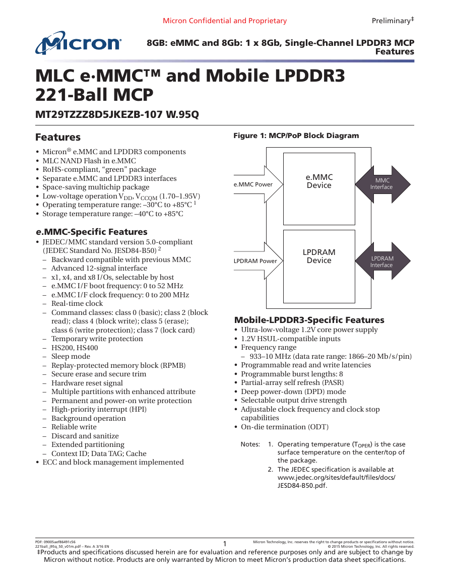
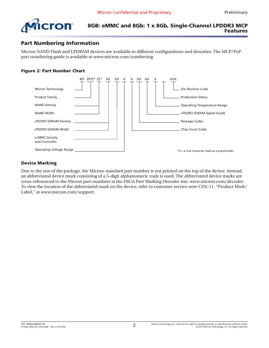
Micron Confidential and Proprietary Preliminary‡ 8GB: eMMC and 8Gb: 1 x 8Gb, Single-Channel LPDDR3 MCP Features MLC e·MMC™ and Mobile LPDDR3 221-Ball MCP MT29TZZZ8D5JKEZB-107 W.95Q Features • Micron® e.MMC and LPDDR3 components • MLC NAND Flash in e.MMC • RoHS-compliant, “green” package • Separate e.MMC and LPDDR3 interfaces • Space-saving multichip package • Low-voltage operation VDD, VCCQM (1.70–1.95V) • Operating temperature range: –30°C to +85°C 1 • Storage temperature range: –40°C to +85°C e.MMC-Specific Features • JEDEC/MMC standard version 5.0-compliant (JEDEC Standard No. JESD84-B50) 2 – Backward compatible with previous MMC – Advanced 12-signal interface – x1, x4, and x8 I/Os, selectable by host – e.MMC I/F boot frequency: 0 to 52 MHz – e.MMC I/F clock frequency: 0 to 200 MHz – Real-time clock – Command classes: class 0 (basic); class 2 (block read); class 4 (block write); class 5 (erase); class 6 (write protection); class 7 (lock card) – Temporary write protection – HS200, HS400 – Sleep mode – Replay-protected memory block (RPMB) – Secure erase and secure trim – Hardware reset signal – Multiple partitions with enhanced attribute – Permanent and power-on write protection – High-priority interrupt (HPI) – Background operation – Reliable write – Discard and sanitize – Extended partitioning – Context ID; Data TAG; Cache • ECC and block management implemented Figure 1: MCP/PoP Block Diagram e.MMC Power e.MMC Device MMC Interface LPDRAM Power LPDRAM Device LPDRAM Interface Mobile-LPDDR3-Specific Features • Ultra-low-voltage 1.2V core power supply • 1.2V HSUL-compatible inputs • Frequency range – 933–10 MHz (data rate range: 1866–20 Mb/s/pin) • Programmable read and write latencies • Programmable burst lengths: 8 • Partial-array self refresh (PASR) • Deep power-down (DPD) mode • Selectable output drive strength • Adjustable clock frequency and clock stop capabilities • On-die termination (ODT) Notes: 1. Operating temperature (TOPER) is the case surface temperature on the center/top of the package. 2. The JEDEC specification is available at www.jedec.org/sites/default/files/docs/ JESD84-B50.pdf. PDF: 09005aef86491c56 Micron Technology, Inc. reserves the right to change products or specifications without notice. 221ball_j95q_50_v01m.pdf – Rev. A 3/16 EN © 2015 Micron Technology, Inc. All rights reserved. ‡Products and specifications discussed herein are for evaluation and reference purposes only and are subject to change by Micron without notice. Products are only warranted by Micron to meet Micron’s production data sheet specifications. 1
Micron Confidential and Proprietary Preliminary 8GB: eMMC and 8Gb: 1 x 8Gb, Single-Channel LPDDR3 MCP Features Part Numbering Information Micron NAND Flash and LPDRAM devices are available in different configurations and densities. The MCP/PoP part numbering guide is available at www.micron.com/numbering. Figure 2: Part Number Chart MT 29TZ* ZZ* XX XX X X XX -XX X .XXX Micron Technology Product Family NAND Density NAND Width LPDDR3 SDRAM Density LPDDR3 SDRAM Width e.MMC Density and Controller Operating Voltage Range Device Marking Die Revision Code Production Status Operating Temperature Range LPDDR3 SDRAM Speed Grade Package Codes Chip Count Code *Z = a null character used as a placeholder. Due to the size of the package, the Micron-standard part number is not printed on the top of the device. Instead, an abbreviated device mark consisting of a 5-digit alphanumeric code is used. The abbreviated device marks are cross-referenced to the Micron part numbers at the FBGA Part Marking Decoder site: www.micron.com/decoder. To view the location of the abbreviated mark on the device, refer to customer service note CSN-11, “Product Mark/ Label,” at www.micron.com/support. PDF: 09005aef86491c56 221ball_j95q_50_v01m.pdf – Rev. A 3/16 EN 2 Micron Technology, Inc. reserves the right to change products or specifications without notice. © 2015 Micron Technology, Inc. All rights reserved.
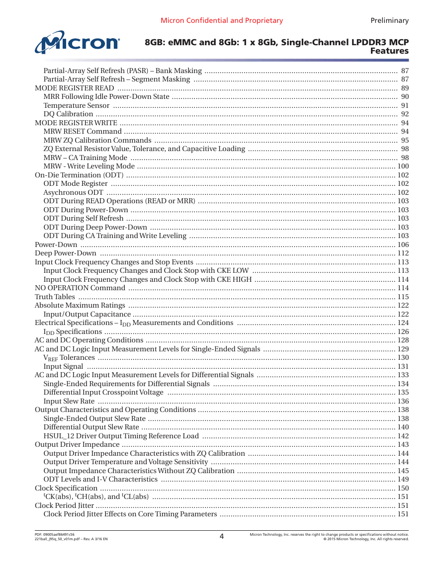
Micron Confidential and Proprietary Preliminary 8GB: eMMC and 8Gb: 1 x 8Gb, Single-Channel LPDDR3 MCP Features Contents MCP General Description ............................................................................................................................... 11 Ball Assignments ............................................................................................................................................ 12 Ball Descriptions ............................................................................................................................................ 13 Device Diagrams ............................................................................................................................................ 15 Package Dimensions ....................................................................................................................................... 16 8GB e·MMC™ Memory .................................................................................................................................. 17 CID Register ............................................................................................................................................... 17 OCR Register .................................................................................................................................................. 18 CSD Register .................................................................................................................................................. 19 ECSD Register ................................................................................................................................................ 21 e.MMC Performance and Current Consumption .............................................................................................. 28 Architecture ................................................................................................................................................... 29 MMC Protocol Independent of NAND Flash Technology .............................................................................. 29 Defect and Error Management .................................................................................................................... 29 State Diagrams ............................................................................................................................................... 30 Electrical Specifications .................................................................................................................................. 34 e.MMC Electrical Specifications .................................................................................................................. 34 LPDDR3 Electrical Specifications ................................................................................................................ 34 DC Electrical Specifications – Device Power ..................................................................................................... 34 8Gb: x16, x32 Mobile LPDDR3 SDRAM ............................................................................................................ 37 Features ..................................................................................................................................................... 37 LPDDR3 Array Configuration .......................................................................................................................... 38 LPDDR3 MR0, MR5, MR6, MR8 Readout ......................................................................................................... 38 IDD Specifications – Single Die ......................................................................................................................... 39 Functional Description ................................................................................................................................... 43 Simplified Bus Interface State Diagram ............................................................................................................ 45 Power-Up and Initialization ............................................................................................................................ 47 Voltage Ramp and Device Initialization ....................................................................................................... 47 Initialization After Reset (Without Voltage Ramp) ........................................................................................ 49 Power-Off Sequence ....................................................................................................................................... 50 Uncontrolled Power-Off Sequence .............................................................................................................. 50 Standard Mode Register Definition .................................................................................................................. 51 Mode Register Assignments and Definitions ................................................................................................ 51 Commands and Timing .................................................................................................................................. 61 ACTIVATE Command ..................................................................................................................................... 62 8-Bank Device Operation ............................................................................................................................ 62 Read and Write Access Modes ......................................................................................................................... 63 Burst READ Command ................................................................................................................................... 64 tDQSCK Delta Timing ................................................................................................................................. 66 Burst WRITE Command .................................................................................................................................. 70 Write Data Mask ............................................................................................................................................. 74 PRECHARGE Command ................................................................................................................................. 75 Burst READ Operation Followed by PRECHARGE ......................................................................................... 76 Burst WRITE Followed by PRECHARGE ....................................................................................................... 77 Auto Precharge ........................................................................................................................................... 78 Burst READ with Auto Precharge ................................................................................................................. 78 Burst WRITE with Auto Precharge ............................................................................................................... 79 REFRESH Command ...................................................................................................................................... 81 REFRESH Requirements ............................................................................................................................. 84 SELF REFRESH Operation ............................................................................................................................... 86 PDF: 09005aef86491c56 221ball_j95q_50_v01m.pdf – Rev. A 3/16 EN 3 Micron Technology, Inc. reserves the right to change products or specifications without notice. © 2015 Micron Technology, Inc. All rights reserved.
Micron Confidential and Proprietary Preliminary 8GB: eMMC and 8Gb: 1 x 8Gb, Single-Channel LPDDR3 MCP Features Partial-Array Self Refresh (PASR) – Bank Masking ......................................................................................... 87 Partial-Array Self Refresh – Segment Masking .............................................................................................. 87 MODE REGISTER READ ................................................................................................................................. 89 MRR Following Idle Power-Down State ........................................................................................................ 90 Temperature Sensor ................................................................................................................................... 91 DQ Calibration ........................................................................................................................................... 92 MODE REGISTER WRITE ................................................................................................................................ 94 MRW RESET Command .............................................................................................................................. 94 MRW ZQ Calibration Commands ................................................................................................................ 95 ZQ External Resistor Value, Tolerance, and Capacitive Loading ..................................................................... 98 MRW – CA Training Mode ........................................................................................................................... 98 MRW - Write Leveling Mode ....................................................................................................................... 100 On-Die Termination (ODT) ............................................................................................................................ 102 ODT Mode Register ................................................................................................................................... 102 Asychronous ODT ..................................................................................................................................... 102 ODT During READ Operations (READ or MRR) ........................................................................................... 103 ODT During Power-Down .......................................................................................................................... 103 ODT During Self Refresh ............................................................................................................................ 103 ODT During Deep Power-Down ................................................................................................................. 103 ODT During CA Training and Write Leveling ............................................................................................... 103 Power-Down ................................................................................................................................................. 106 Deep Power-Down ........................................................................................................................................ 112 Input Clock Frequency Changes and Stop Events ............................................................................................ 113 Input Clock Frequency Changes and Clock Stop with CKE LOW .................................................................. 113 Input Clock Frequency Changes and Clock Stop with CKE HIGH ................................................................. 114 NO OPERATION Command ........................................................................................................................... 114 Truth Tables .................................................................................................................................................. 115 Absolute Maximum Ratings ........................................................................................................................... 122 Input/Output Capacitance ......................................................................................................................... 122 Electrical Specifications – IDD Measurements and Conditions ......................................................................... 124 IDD Specifications ...................................................................................................................................... 126 AC and DC Operating Conditions ................................................................................................................... 128 AC and DC Logic Input Measurement Levels for Single-Ended Signals ............................................................. 129 VREF Tolerances ......................................................................................................................................... 130 Input Signal .............................................................................................................................................. 131 AC and DC Logic Input Measurement Levels for Differential Signals ................................................................ 133 Single-Ended Requirements for Differential Signals .................................................................................... 134 Differential Input Crosspoint Voltage ......................................................................................................... 135 Input Slew Rate ......................................................................................................................................... 136 Output Characteristics and Operating Conditions ........................................................................................... 138 Single-Ended Output Slew Rate .................................................................................................................. 138 Differential Output Slew Rate ..................................................................................................................... 140 HSUL_12 Driver Output Timing Reference Load ......................................................................................... 142 Output Driver Impedance .............................................................................................................................. 143 Output Driver Impedance Characteristics with ZQ Calibration .................................................................... 144 Output Driver Temperature and Voltage Sensitivity ..................................................................................... 144 Output Impedance Characteristics Without ZQ Calibration ......................................................................... 145 ODT Levels and I-V Characteristics ............................................................................................................ 149 Clock Specification ........................................................................................................................................ 150 tCK(abs), tCH(abs), and tCL(abs) ................................................................................................................ 151 Clock Period Jitter .......................................................................................................................................... 151 Clock Period Jitter Effects on Core Timing Parameters ................................................................................. 151 PDF: 09005aef86491c56 221ball_j95q_50_v01m.pdf – Rev. A 3/16 EN 4 Micron Technology, Inc. reserves the right to change products or specifications without notice. © 2015 Micron Technology, Inc. All rights reserved.
Micron Confidential and Proprietary Preliminary 8GB: eMMC and 8Gb: 1 x 8Gb, Single-Channel LPDDR3 MCP Features Cycle Time Derating for Core Timing Parameters ........................................................................................ 152 Clock Cycle Derating for Core Timing Parameters ....................................................................................... 152 Clock Jitter Effects on Command/Address Timing Parameters ..................................................................... 152 Clock Jitter Effects on Read Timing Parameters ........................................................................................... 152 Clock Jitter Effects on Write Timing Parameters .......................................................................................... 153 Refresh Requirements .................................................................................................................................... 154 AC Timing ..................................................................................................................................................... 155 CA and CS_n Setup, Hold, and Derating .......................................................................................................... 162 Data Setup, Hold, and Slew Rate Derating ....................................................................................................... 169 Revision History ............................................................................................................................................ 176 Rev. A – 03/16 ............................................................................................................................................ 176 PDF: 09005aef86491c56 221ball_j95q_50_v01m.pdf – Rev. A 3/16 EN 5 Micron Technology, Inc. reserves the right to change products or specifications without notice. © 2015 Micron Technology, Inc. All rights reserved.
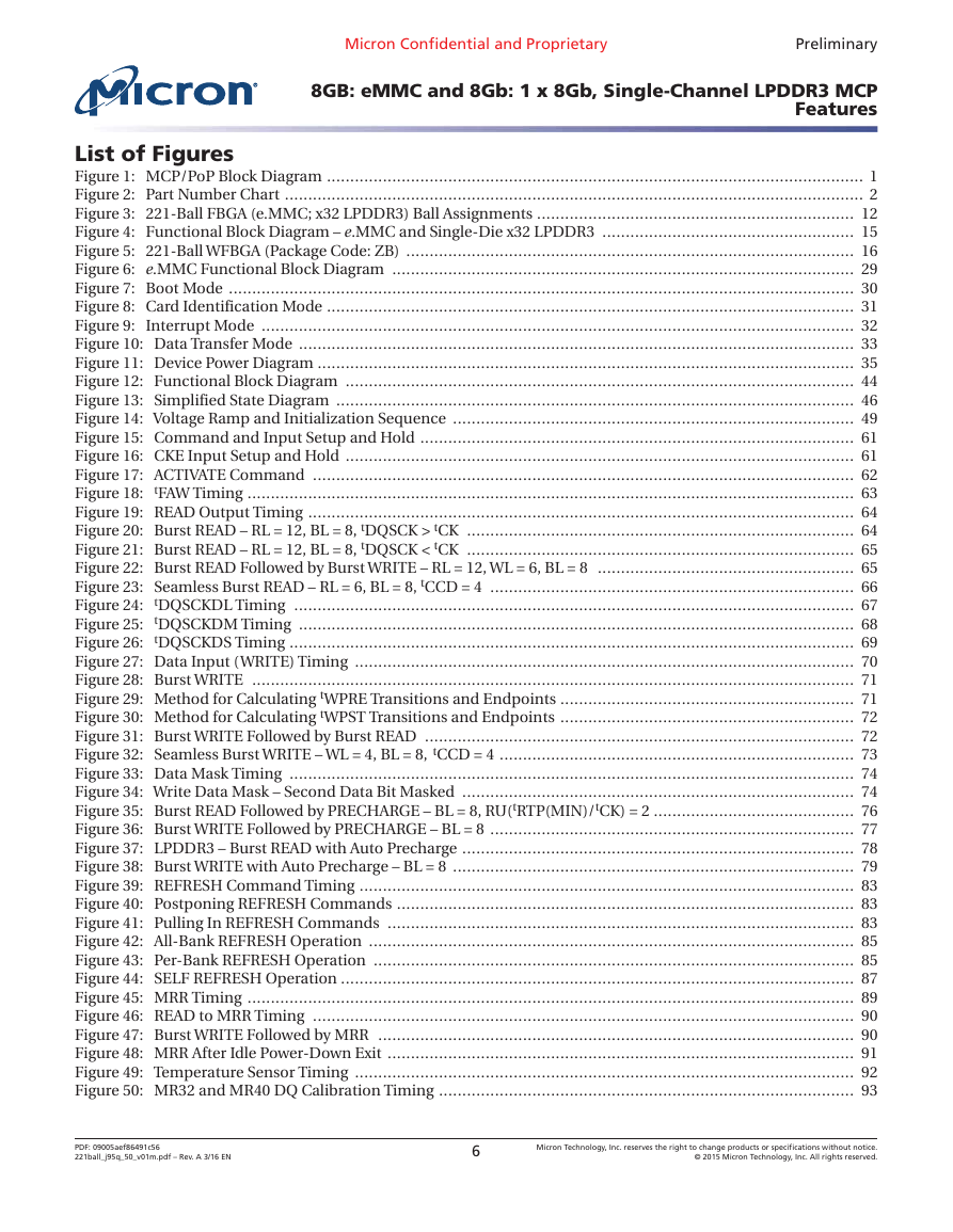
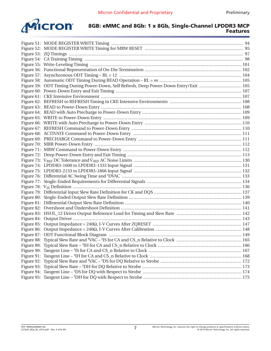
Micron Confidential and Proprietary Preliminary 8GB: eMMC and 8Gb: 1 x 8Gb, Single-Channel LPDDR3 MCP Features List of Figures Figure 1: MCP/PoP Block Diagram ................................................................................................................... 1 Figure 2: Part Number Chart ............................................................................................................................ 2 Figure 3: 221-Ball FBGA (e.MMC; x32 LPDDR3) Ball Assignments .................................................................... 12 Figure 4: Functional Block Diagram – e.MMC and Single-Die x32 LPDDR3 ...................................................... 15 Figure 5: 221-Ball WFBGA (Package Code: ZB) ................................................................................................ 16 Figure 6: e.MMC Functional Block Diagram ................................................................................................... 29 Figure 7: Boot Mode ...................................................................................................................................... 30 Figure 8: Card Identification Mode ................................................................................................................. 31 Figure 9: Interrupt Mode ............................................................................................................................... 32 Figure 10: Data Transfer Mode ....................................................................................................................... 33 Figure 11: Device Power Diagram ................................................................................................................... 35 Figure 12: Functional Block Diagram ............................................................................................................. 44 Figure 13: Simplified State Diagram ............................................................................................................... 46 Figure 14: Voltage Ramp and Initialization Sequence ...................................................................................... 49 Figure 15: Command and Input Setup and Hold ............................................................................................. 61 Figure 16: CKE Input Setup and Hold ............................................................................................................. 61 Figure 17: ACTIVATE Command .................................................................................................................... 62 Figure 18: tFAW Timing .................................................................................................................................. 63 Figure 19: READ Output Timing ..................................................................................................................... 64 Figure 20: Burst READ – RL = 12, BL = 8, tDQSCK > tCK ................................................................................... 64 Figure 21: Burst READ – RL = 12, BL = 8, tDQSCK < tCK ................................................................................... 65 Figure 22: Burst READ Followed by Burst WRITE – RL = 12, WL = 6, BL = 8 ....................................................... 65 Figure 23: Seamless Burst READ – RL = 6, BL = 8, tCCD = 4 .............................................................................. 66 Figure 24: tDQSCKDL Timing ........................................................................................................................ 67 Figure 25: tDQSCKDM Timing ....................................................................................................................... 68 Figure 26: tDQSCKDS Timing ......................................................................................................................... 69 Figure 27: Data Input (WRITE) Timing ........................................................................................................... 70 Figure 28: Burst WRITE ................................................................................................................................. 71 Figure 29: Method for Calculating tWPRE Transitions and Endpoints ............................................................... 71 Figure 30: Method for Calculating tWPST Transitions and Endpoints ............................................................... 72 Figure 31: Burst WRITE Followed by Burst READ ............................................................................................ 72 Figure 32: Seamless Burst WRITE – WL = 4, BL = 8, tCCD = 4 ............................................................................ 73 Figure 33: Data Mask Timing ......................................................................................................................... 74 Figure 34: Write Data Mask – Second Data Bit Masked .................................................................................... 74 Figure 35: Burst READ Followed by PRECHARGE – BL = 8, RU(tRTP(MIN)/tCK) = 2 ........................................... 76 Figure 36: Burst WRITE Followed by PRECHARGE – BL = 8 .............................................................................. 77 Figure 37: LPDDR3 – Burst READ with Auto Precharge .................................................................................... 78 Figure 38: Burst WRITE with Auto Precharge – BL = 8 ...................................................................................... 79 Figure 39: REFRESH Command Timing .......................................................................................................... 83 Figure 40: Postponing REFRESH Commands .................................................................................................. 83 Figure 41: Pulling In REFRESH Commands .................................................................................................... 83 Figure 42: All-Bank REFRESH Operation ........................................................................................................ 85 Figure 43: Per-Bank REFRESH Operation ....................................................................................................... 85 Figure 44: SELF REFRESH Operation .............................................................................................................. 87 Figure 45: MRR Timing .................................................................................................................................. 89 Figure 46: READ to MRR Timing .................................................................................................................... 90 Figure 47: Burst WRITE Followed by MRR ...................................................................................................... 90 Figure 48: MRR After Idle Power-Down Exit .................................................................................................... 91 Figure 49: Temperature Sensor Timing ........................................................................................................... 92 Figure 50: MR32 and MR40 DQ Calibration Timing ......................................................................................... 93 PDF: 09005aef86491c56 221ball_j95q_50_v01m.pdf – Rev. A 3/16 EN 6 Micron Technology, Inc. reserves the right to change products or specifications without notice. © 2015 Micron Technology, Inc. All rights reserved.
Micron Confidential and Proprietary Preliminary 8GB: eMMC and 8Gb: 1 x 8Gb, Single-Channel LPDDR3 MCP Features Figure 51: MODE REGISTER WRITE Timing ................................................................................................... 94 Figure 52: MODE REGISTER WRITE Timing for MRW RESET .......................................................................... 95 Figure 53: ZQ Timings ................................................................................................................................... 97 Figure 54: CA Training Timing ....................................................................................................................... 98 Figure 55: Write-Leveling Timing .................................................................................................................. 101 Figure 56: Functional Representation of On-Die Termination ......................................................................... 102 Figure 57: Asynchronous ODT Timing – RL = 12 ............................................................................................ 104 Figure 58: Automatic ODT Timing During READ Operation – RL = m .............................................................. 105 Figure 59: ODT Timing During Power-Down, Self Refresh, Deep Power-Down Entry/Exit ................................ 105 Figure 60: Power-Down Entry and Exit Timing ............................................................................................... 107 Figure 61: CKE Intensive Environment .......................................................................................................... 107 Figure 62: REFRESH to REFRESH Timing in CKE Intensive Environments ...................................................... 108 Figure 63: READ to Power-Down Entry .......................................................................................................... 108 Figure 64: READ with Auto Precharge to Power-Down Entry ........................................................................... 109 Figure 65: WRITE to Power-Down Entry ........................................................................................................ 109 Figure 66: WRITE with Auto Precharge to Power-Down Entry ......................................................................... 110 Figure 67: REFRESH Command to Power-Down Entry ................................................................................... 110 Figure 68: ACTIVATE Command to Power-Down Entry .................................................................................. 111 Figure 69: PRECHARGE Command to Power-Down Entry .............................................................................. 111 Figure 70: MRR Power-Down Entry ............................................................................................................... 112 Figure 71: MRW Command to Power-Down Entry ......................................................................................... 112 Figure 72: Deep Power-Down Entry and Exit Timing ...................................................................................... 113 Figure 73: VREF DC Tolerance and V REF AC Noise Limits ................................................................................. 130 Figure 74: LPDDR3-1600 to LPDDR3-1333 Input Signal ................................................................................. 131 Figure 75: LPDDR3-2133 to LPDDR3-1866 Input Signal ................................................................................. 132 Figure 76: Differential AC Swing Time and tDVAC .......................................................................................... 133 Figure 77: Single-Ended Requirements for Differential Signals ....................................................................... 134 Figure 78: VIX Definition ............................................................................................................................... 136 Figure 79: Differential Input Slew Rate Definition for CK and DQS .................................................................. 137 Figure 80: Single-Ended Output Slew Rate Definition ..................................................................................... 139 Figure 81: Differential Output Slew Rate Definition ........................................................................................ 140 Figure 82: Overshoot and Undershoot Definition ........................................................................................... 141 Figure 83: HSUL_12 Driver Output Reference Load for Timing and Slew Rate ................................................. 142 Figure 84: Output Driver ............................................................................................................................... 143 Figure 85: Output Impedance = 240Ω, I-V Curves After ZQRESET ................................................................... 147 Figure 86: Output Impedance = 240Ω, I-V Curves After Calibration ................................................................. 148 Figure 87: ODT Functional Block Diagram .................................................................................................... 149 Figure 88: Typical Slew Rate and tVAC – tIS for CA and CS_n Relative to Clock ................................................. 165 Figure 89: Typical Slew Rate – tIH for CA and CS_n Relative to Clock ............................................................... 166 Figure 90: Tangent Line – tIS for CA and CS_n Relative to Clock ...................................................................... 167 Figure 91: Tangent Line – tIH for CA and CS_n Relative to Clock ..................................................................... 168 Figure 92: Typical Slew Rate and tVAC – tDS for DQ Relative to Strobe ............................................................. 172 Figure 93: Typical Slew Rate – tDH for DQ Relative to Strobe ........................................................................... 173 Figure 94: Tangent Line – tDS for DQ with Respect to Strobe .......................................................................... 174 Figure 95: Tangent Line – tDH for DQ with Respect to Strobe .......................................................................... 175 PDF: 09005aef86491c56 221ball_j95q_50_v01m.pdf – Rev. A 3/16 EN 7 Micron Technology, Inc. reserves the right to change products or specifications without notice. © 2015 Micron Technology, Inc. All rights reserved.
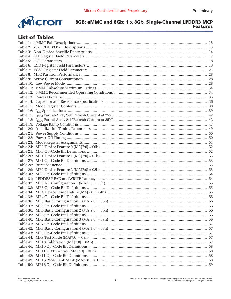
Micron Confidential and Proprietary Preliminary 8GB: eMMC and 8Gb: 1 x 8Gb, Single-Channel LPDDR3 MCP Features List of Tables Table 1: e.MMC Ball Descriptions ................................................................................................................... 13 Table 2: x32 LPDDR3 Ball Descriptions ........................................................................................................... 13 Table 3: Non-Device-Specific Descriptions ..................................................................................................... 14 Table 4: CID Register Field Parameters ........................................................................................................... 17 Table 5: OCR Parameters ............................................................................................................................... 18 Table 6: CSD Register Field Parameters .......................................................................................................... 19 Table 7: ECSD Register Field Parameters ........................................................................................................ 21 Table 8: MLC Partition Performance ............................................................................................................... 28 Table 9: Active Current Consumption ............................................................................................................. 28 Table 10: Low Power Mode ............................................................................................................................ 28 Table 11: e.MMC Absolute Maximum Ratings ................................................................................................. 34 Table 12: e.MMC Recommended Operating Conditions .................................................................................. 34 Table 13: Power Domains .............................................................................................................................. 35 Table 14: Capacitor and Resistance Specifications .......................................................................................... 36 Table 15: Mode Register Contents .................................................................................................................. 38 Table 16: IDD Specifications ........................................................................................................................... 39 Table 17: IDD6 Partial-Array Self Refresh Current at 25°C .................................................................................. 42 Table 18: IDD6 Partial-Array Self Refresh Current at 85°C .................................................................................. 42 Table 19: Voltage Ramp Conditions ................................................................................................................ 47 Table 20: Initialization Timing Parameters ...................................................................................................... 49 Table 21: Power Supply Conditions ................................................................................................................ 50 Table 22: Power-Off Timing ............................................................................................................................ 50 Table 23: Mode Register Assignments ............................................................................................................. 51 Table 24: MR0 Device Feature 0 (MA[7:0] = 00h) .............................................................................................. 52 Table 25: MR0 Op-Code BIt Definitions .......................................................................................................... 52 Table 26: MR1 Device Feature 1 (MA[7:0] = 01h) .............................................................................................. 53 Table 27: MR1 Op-Code Bit Definitions .......................................................................................................... 53 Table 28: Burst Sequence ............................................................................................................................... 53 Table 29: MR2 Device Feature 2 (MA[7:0] = 02h) .............................................................................................. 53 Table 30: MR2 Op-Code Bit Definitions .......................................................................................................... 54 Table 31: LPDDR3 READ and WRITE Latency ................................................................................................. 54 Table 32: MR3 I/O Configuration 1 (MA[7:0] = 03h) ......................................................................................... 55 Table 33: MR3 Op-Code Bit Definitions .......................................................................................................... 55 Table 34: MR4 Device Temperature (MA[7:0] = 04h) ........................................................................................ 55 Table 35: MR4 Op-Code Bit Definitions .......................................................................................................... 55 Table 36: MR5 Basic Configuration 1 (MA[7:0] = 05h) ...................................................................................... 56 Table 37: MR5 Op-Code Bit Definitions .......................................................................................................... 56 Table 38: MR6 Basic Configuration 2 (MA[7:0] = 06h) ...................................................................................... 56 Table 39: MR6 Op-Code Bit Definitions .......................................................................................................... 56 Table 40: MR7 Basic Configuration 3 (MA[7:0] = 07h) ...................................................................................... 56 Table 41: MR7 Op-Code Bit Definitions .......................................................................................................... 57 Table 42: MR8 Basic Configuration 4 (MA[7:0] = 08h) ...................................................................................... 57 Table 43: MR8 Op-Code Bit Definitions .......................................................................................................... 57 Table 44: MR9 Test Mode (MA[7:0] = 09h) ....................................................................................................... 57 Table 45: MR10 Calibration (MA[7:0] = 0Ah) ................................................................................................... 57 Table 46: MR10 Op-Code Bit Definitions ........................................................................................................ 58 Table 47: MR11 ODT Control (MA[7:0] = 0Bh) ................................................................................................. 58 Table 48: MR11 Op-Code Bit Definitions ........................................................................................................ 58 Table 49: MR16 PASR Bank Mask (MA[7:0] = 010h) .......................................................................................... 58 Table 50: MR16 Op-Code Bit Definitions ........................................................................................................ 59 PDF: 09005aef86491c56 221ball_j95q_50_v01m.pdf – Rev. A 3/16 EN 8 Micron Technology, Inc. reserves the right to change products or specifications without notice. © 2015 Micron Technology, Inc. All rights reserved.
分享到:
收藏