logo资料库

ls1043的技术手册.pdf

第1页 / 共260页
第2页 / 共260页
第3页 / 共260页
第4页 / 共260页
第5页 / 共260页
第6页 / 共260页
第7页 / 共260页
第8页 / 共260页
资料共260页,剩余部分请下载后查看
Features
Introduction
Pin assignments
621 ball layout diagrams
Pinout list (21x21)
780 ball layout diagrams
Pinout list
Electrical characteristics
Overall DC electrical characteristics
Absolute maximum ratings
Recommended operating conditions
Output driver characteristics
General AC timing specifications
Power sequencing
Power down requirements
Power characteristics
Low power mode saving estimation
I/O power dissipation
Power-on ramp rate
Input clocks
System clock (SYSCLK)
SYSCLK DC electrical characteristics
SYSCLK AC timing specifications
Spread-spectrum sources
Real-time clock timing (RTC)
Gigabit Ethernet reference clock timing
DDR clock (DDRCLK)
DDRCLK DC electrical characteristics
DDRCLK AC timing specifications
Differential system clock (DIFF_SYSCLK/DIFF_SYSCLK_B) timing specifications
Differential system clock DC timing characteristics
Differential system clock AC timing specifications
Other input clocks
RESET initialization
DDR4 and DDR3L SDRAM controller
DDR4 and DDR3L SDRAM interface DC electrical characteristics
DDR4 and DDR3L SDRAM interface AC timing specifications
DDR4 and DDR3L SDRAM interface input AC timing specifications
DDR4 and DDR3L SDRAM interface output AC timing specifications
Ethernet interface, Ethernet management interface, IEEE Std 1588
SGMII interface
SGMII clocking requirements for SD1_REF_CLKn_P and SD1_REF_CLKn_N
SGMII DC electrical characteristics
SGMII and SGMII 2.5G transmit DC specifications
SGMII and SGMII 2.5G DC receiver electrical characteristics
SGMII AC timing specifications
SGMII and SGMII 2.5G transmit AC timing specifications
SGMII AC measurement details
SGMII and SGMII 2.5G receiver AC timing Specification
QSGMII interface
QSGMII clocking requirements for SD1_REF_CLKn_P and SD1_REF_CLKn_N
QSGMII DC electrical characteristics
QSGMII transmitter DC specifications
QSGMII DC receiver electrical characteristics
QSGMII AC timing specifications
QSGMII transmit AC timing specifications
QSGMII receiver AC timing Specification
XFI interface
XFI clocking requirements for SD1_REF_CLKn_P and SD1_REF_CLKn_N
XFI DC electrical characteristics
XFI transmitter DC electrical characteristics
XFI receiver DC electrical characteristics
XFI AC timing specifications
XFI transmitter AC timing specifications
XFI receiver AC timing specifications
1000Base-KX interface
1000Base-KX DC electrical characteristics
1000Base-KX Transmitter DC Specifications
1000Base-KX Receiver DC Specifications
1000Base-KX AC electrical characteristics
1000Base-KX Transmitter AC Specifications
1000Base-KX Receiver AC Specifications
RGMII electrical specifications
RGMII DC electrical characteristics
RGMII AC timing specifications
Ethernet management interface (EMI)
Ethernet management interface 1 (EMI1)
EMI1 DC electrical characteristics
EMI1 AC timing specifications
Ethernet management interface 2 (EMI2)
EMI2 DC electrical characteristics
EMI2 AC timing specifications
IEEE 1588 electrical specifications
IEEE 1588 DC electrical characteristics
IEEE 1588 AC timing specifications
QUICC engine specifications
HDLC interface
HDLC and Synchronous UART DC electrical characteristics
HDLC and Synchronous UART AC timing specifications
Time-division-multiplexed and serial interface (TDM/SI)
TDM/SI DC electrical characteristics
TDM/SI AC timing specifications
USB 3.0 interface
USB 3.0 PHY transceiver supply DC voltage
USB 3.0 DC electrical characteristics
USB 3.0 AC timing specifications
USB 3.0 reference clock requirements
USB 3.0 LFPS specifications
Integrated Flash Controller
IFC DC electrical characteristics
Integrated Flash Controller AC Timing Specifications
Test Condition
IFC AC Timing Specifications (GPCM/GASIC)
IFC AC Timing Specifications (NOR)
IFC AC Timing Specifications (NAND)
IFC-NAND SDR AC Timing Specifications
IFC-NAND NVDDR AC Timing Specification
LPUART interface
LPUART DC electrical characteristics
LPUART AC timing specifications
DUART interface
DUART DC electrical characteristics
DUART AC timing specifications
Flextimer interface
Flextimer DC electrical characteristics
Flextimer AC timing specifications
SPI interface
SPI DC electrical characteristics
SPI AC timing specifications
QuadSPI interface
QuadSPI DC electrical characteristics
QuadSPI AC timing specifications
QuadSPI timing SDR mode
Enhanced secure digital host controller (eSDHC)
eSDHC DC electrical characteristics
eSDHC AC timing specifications
JTAG controller
JTAG DC electrical characteristics
JTAG AC timing specifications
I2C interface
I2C DC electrical characteristics
I2C AC timing specifications
GPIO interface
GPIO DC electrical characteristics
GPIO AC timing specifications
GIC interface
GIC DC electrical characteristics
GIC AC timing specifications
High-speed serial interfaces (HSSI)
Signal terms definitions
SerDes reference clocks
SerDes spread-spectrum clock source recommendations
SerDes reference clock receiver characteristics
DC-level requirements for SerDes reference clocks
AC requirements for SerDes reference clocks
SerDes transmitter and receiver reference circuits
PCI Express
Clocking dependencies
PCI Express DC physical layer specifications
PCI Express DC physical layer transmitter specifications
PCI Express DC physical layer receiver specifications
PCI Express AC physical layer specifications
PCI Express AC physical layer transmitter specifications
PCI Express AC physical layer receiver specifications
Test and measurement load
Serial ATA (SATA) interface
SATA DC electrical characteristics
SATA DC transmitter output characteristics
SATA DC receiver input characteristics
SATA AC timing specifications
AC requirements for SATA REF_CLK
AC transmitter output characteristics
AC differential receiver input characteristics
Hardware design considerations
System clocking
PLL characteristics
Clock ranges
DDR clock ranges
Platform to SYSCLK PLL ratio
Core cluster to SYSCLK PLL ratio
Core complex PLL select
DDR controller PLL ratios
Valid reference clocks and PLL configurations for SerDes protocols
Frequency options
SYSCLK and core cluster frequency options
SYSCLK and platform frequency options
DDRCLK and DDR data rate frequency options
SYSCLK and eSDHC high speed modes frequency options
Minimum platform frequency requirements for high-speed interfaces
Connection recommendations
JTAG configuration signals
Termination of unused signals
Guidelines for high-speed interface termination
SerDes interface entirely unused
SerDes interface partly unused
Thermal
Recommended thermal model
Temperature diode
Thermal management information
Internal package conduction resistance
Thermal interface materials
Package information
Package parameters for the FC-PBGA
Mechanical dimensions of the FC-PBGA
Security fuse processor
Ordering information
Part numbering nomenclature
Part marking
Revision history
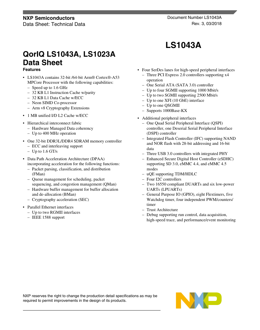
NXP Semiconductors Data Sheet: Technical Data QorIQ LS1043A, LS1023A Data Sheet Features • LS1043A contains 32-bit /64-bit Arm® Cortex®-A53 MPCore Processor with the following capabilities: – Speed up to 1.6 GHz – 32 KB L1 Instruction Cache w/parity – 32 KB L1 Data Cache w/ECC – Neon SIMD Co-processor – Arm v8 Cryptography Extensions • 1 MB unified I/D L2 Cache w/ECC • Hierarchical interconnect fabric – Hardware Managed Data coherency – Up to 400 MHz operation • One 32-bit DDR3L/DDR4 SDRAM memory controller – ECC and interleaving support – Up to 1.6 GT/s • Data Path Acceleration Architecture (DPAA) incorporating acceleration for the following functions: – Packet parsing, classification, and distribution (FMan) – Queue management for scheduling, packet sequencing, and congestion management (QMan) – Hardware buffer management for buffer allocation and de-allocation (BMan) – Cryptography acceleration (SEC) • Parallel Ethernet interfaces – Up to two RGMII interfaces – IEEE 1588 support Document Number LS1043A Rev. 3, 03/2018 LS1043A • Four SerDes lanes for high-speed peripheral interfaces – Three PCI Express 2.0 controllers supporting x4 operation – One Serial ATA (SATA 3.0) controller – Up to four SGMII supporting 1000 Mbit/s – Up to two SGMII supporting 2500 Mbit/s – Up to one XFI (10 GbE) interface – Up to one QSGMII – Supports 1000Base-KX • Additional peripheral interfaces – One Quad Serial Peripheral Interface (QSPI) controller, one Deserial Serial Peripheral Interface (DSPI) controller – Integrated Flash Controller (IFC) supporting NAND and NOR flash with 28-bit addressing and 16-bit data – Three USB 3.0 controllers with integrated PHY – Enhanced Secure Digital Host Controller (eSDHC) supporting SD 3.0, eMMC 4.4, and eMMC 4.5 modes – uQE supporting TDM/HDLC – Four I2C controllers – Two 16550 compliant DUARTs and six low-power UARTs (LPUARTs) – General Purpose IO (GPIO), eight Flextimers, five Watchdog timer, four independent PWM/counters/ timer – Trust Architecture – Debug supporting run control, data acquisition, high-speed trace, and performance/event monitoring NXP reserves the right to change the production detail specifications as may be required to permit improvements in the design of its products.
Table of Contents 1 Introduction.......................................................................................... 3 3.17 Flextimer interface.....................................................................182 2 Pin assignments.................................................................................... 4 3.18 SPI interface.............................................................................. 185 2.1 2.2 2.3 2.4 621 ball layout diagrams........................................................... 4 3.19 QuadSPI interface......................................................................187 Pinout list (21x21)..................................................................... 10 3.20 Enhanced secure digital host controller (eSDHC).....................189 780 ball layout diagrams........................................................... 48 3.21 JTAG controller.........................................................................198 Pinout list...................................................................................54 3.22 I2C interface.............................................................................. 201 3 Electrical characteristics.......................................................................96 3.23 GPIO interface...........................................................................204 3.1 3.2 3.3 3.4 3.5 3.6 3.7 3.8 3.9 Overall DC electrical characteristics......................................... 96 3.24 GIC interface............................................................................. 208 Power sequencing......................................................................104 3.25 High-speed serial interfaces (HSSI).......................................... 210 Power down requirements......................................................... 107 4 Hardware design considerations...........................................................232 Power characteristics................................................................. 107 Low power mode saving estimation..........................................110 4.1 4.2 System clocking........................................................................ 233 Connection recommendations................................................... 242 I/O power dissipation................................................................ 111 5 Thermal................................................................................................ 247 Power-on ramp rate................................................................... 113 Input clocks............................................................................... 114 RESET initialization..................................................................120 5.1 5.2 5.3 Recommended thermal model...................................................249 Temperature diode.....................................................................249 Thermal management information............................................ 249 3.10 DDR4 and DDR3L SDRAM controller.................................... 121 6 Package information.............................................................................252 3.11 Ethernet interface, Ethernet management interface, IEEE Std 6.1 Package parameters for the FC-PBGA......................................252 1588........................................................................................... 128 6.2 Mechanical dimensions of the FC-PBGA................................. 252 3.12 QUICC engine specifications.................................................... 153 7 Security fuse processor.........................................................................255 3.13 USB 3.0 interface...................................................................... 158 8 Ordering information............................................................................255 3.14 Integrated Flash Controller........................................................161 3.15 LPUART interface.....................................................................179 8.1 8.2 Part numbering nomenclature....................................................255 Part marking ............................................................................. 256 3.16 DUART interface...................................................................... 181 9 Revision history....................................................................................257 2 NXP Semiconductors QorIQ LS1043A, LS1023A Data Sheet, Rev. 3, 03/2018
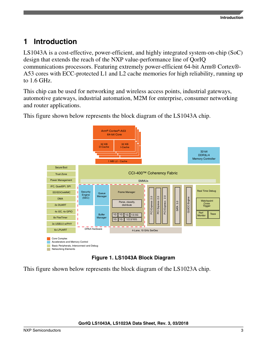
Introduction 1 Introduction LS1043A is a cost-effective, power-efficient, and highly integrated system-on-chip (SoC) design that extends the reach of the NXP value-performance line of QorIQ communications processors. Featuring extremely power-efficient 64-bit Arm® Cortex®- A53 cores with ECC-protected L1 and L2 cache memories for high reliability, running up to 1.6 GHz. This chip can be used for networking and wireless access points, industrial gateways, automotive gateways, industrial automation, M2M for enterprise, consumer networking and router applications. This figure shown below represents the block diagram of the LS1043A chip. 64-bit Core Arm® Cortex®-A53 ARM Cortex- ARM Cortex- A53 64b Cores A53 64b Cores ARM Cortex- A53 64b Cores ARM Cortex- 32 KB 32 KB A53 64b Cores 32 KB I-Cache I-Cache I-Cache 32 KB 32 KB 32 KB D-Cache D-Cache D-Cache 32 KB D-Cache 32 KB I-Cache Secure Boot Trust Zone Power Management IFC, QuadSPI, SPI SD/SDIO/eMMC DMA 2x DUART 4x I2C, 4x GPIO 8x FlexTimer 3x USB3.0 w/PHY 6x LPUART 1 MB L2 - Cache CCI-400™ Coherency Fabric SMMUs Security Engine (SEC) Queue Manager Frame Manager Parse, classify, distribute Buffer Manager 1G 1G 1G 1G 1G 1/2.5G 1/2.5/10G 0 2 . s s e r p x E I C P 0 2 . s s e r p x E I C P 0 . 2 s s e r p x E I C P . 0 3 A T A S DPAA Hardware 4-Lane, 10 GHz SerDes Core Complex Accelerators and Memory Control Basic Peripherals, Interconnect and Debug Networking Elements 32-bit DDR3L/4 Memory Controller Real Time Debug Watchpoint Cross Trigger Perf Monitor Trace i e n g n E C C U Q I This figure shown below represents the block diagram of the LS1023A chip. Figure 1. LS1043A Block Diagram NXP Semiconductors 3 QorIQ LS1043A, LS1023A Data Sheet, Rev. 3, 03/2018
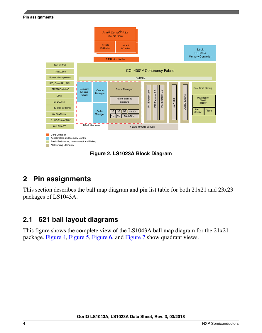
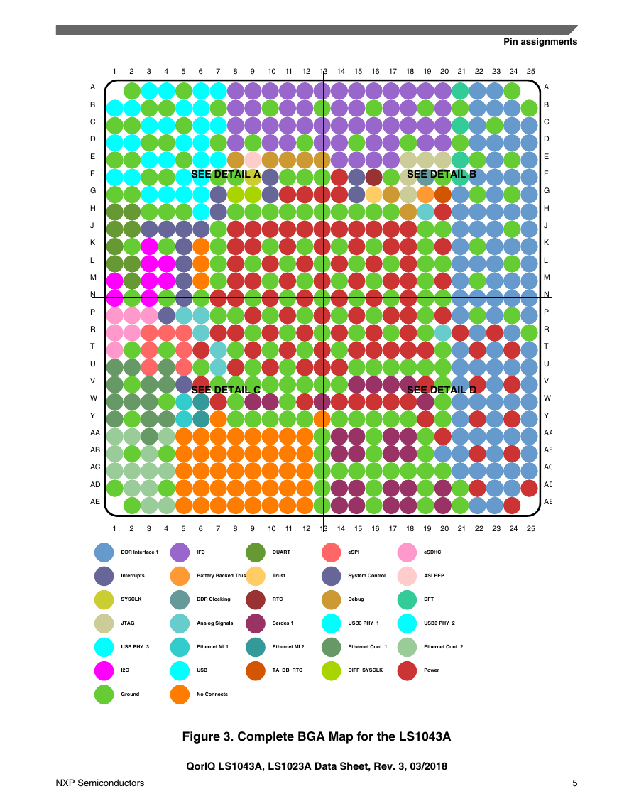
Pin assignments 64-bit Core Arm® Cortex®-A53 ARM Cortex- ARM Cortex- A53 64b Cores A53 64b Cores ARM Cortex- A53 64b Cores ARM Cortex- 32 KB 32 KB A53 64b Cores 32 KB I-Cache 32 KB I-Cache I-Cache I-Cache 32 KB 32 KB 32 KB D-Cache 32 KB D-Cache D-Cache D-Cache Secure Boot Trust Zone Power Management IFC, QuadSPI, SPI SD/SDIO/eMMC DMA 2x DUART 4x I2C, 4x GPIO 8x FlexTimer 3x USB3.0 w/PHY 6x LPUART 1 MB L2 - Cache CCI-400™ Coherency Fabric SMMUs Security Engine (SEC) Queue Manager Frame Manager Parse, classify, distribute Buffer Manager 1G 1G 1G 1G 1G 1/2.5G 1/2.5/10G 0 . 2 s s e r p x E I C P 0 2 . s s e r p x E I C P 0 2 . s s e r p x E I C P 0 3 . A T A S DPAA Hardware 4-Lane 10 GHz SerDes Core Complex Accelerators and Memory Control Basic Peripherals, Interconnect and Debug Networking Elements Figure 2. LS1023A Block Diagram 32-bit DDR3L/4 Memory Controller Real Time Debug Watchpoint Cross Trigger Perf Monitor Trace i e n g n E C C U Q I 2 Pin assignments This section describes the ball map diagram and pin list table for both 21x21 and 23x23 packages of LS1043A. 2.1 621 ball layout diagrams This figure shows the complete view of the LS1043A ball map diagram for the 21x21 package. Figure 4, Figure 5, Figure 6, and Figure 7 show quadrant views. 4 NXP Semiconductors QorIQ LS1043A, LS1023A Data Sheet, Rev. 3, 03/2018
1 2 3 4 5 6 7 8 9 10 11 12 13 14 15 16 17 18 19 20 21 22 23 24 25 Pin assignments A B C D E F G H J K L M N P R T U V W Y AA AB AC AD AE SEE DETAIL A SEE DETAIL B SEE DETAIL C SEE DETAIL D A B C D E F G H J K L M N P R T U V W Y AA AB AC AD AE 1 2 3 4 5 6 7 8 9 10 11 12 13 14 15 16 17 18 19 20 21 22 23 24 25 DDR Interface 1 IFC DUART eSPI eSDHC Interrupts Battery Backed Trust Trust System Control ASLEEP SYSCLK DDR Clocking RTC Debug DFT JTAG Analog Signals Serdes 1 USB3 PHY 1 USB3 PHY 2 USB PHY 3 Ethernet MI 1 Ethernet MI 2 Ethernet Cont. 1 Ethernet Cont. 2 I2C USB TA_BB_RTC DIFF_SYSCLK Power Ground No Connects Figure 3. Complete BGA Map for the LS1043A QorIQ LS1043A, LS1023A Data Sheet, Rev. 3, 03/2018 NXP Semiconductors 5
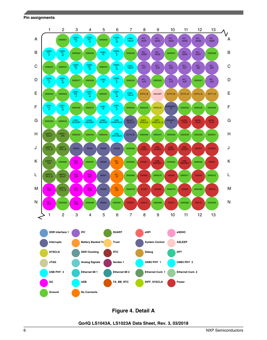
Pin assignments 1 2 3 4 USB3_ RX_ M 5 GND002 USB3_ RX_ P GND001 USB3_ TX_ M USB3_ TX_ P GND004 GND005 USB3_ ID GND013 GND014 USB2_ RX_ P USB2_ RX_ M GND015 USB2_ TX_ P USB2_ TX_ M GND017 GND018 USB2_ ID GND025 GND026 USB1_ RX_ P USB1_ RX_ M GND027 USB1_ TX_ P USB1_ TX_ M GND030 GND031 USB1_ ID A B C D E F G H J K L M N 6 USB3_ D_ M USB3_ D_ P USB2_ D_ M USB2_ D_ P USB1_ D_ M USB1_ D_ P 7 8 9 10 11 12 13 USB3_ VBUS IFC_ AD01 IFC_ AD03 IFC_ AD04 IFC_ AD06 IFC_ AD08 IFC_ AD09 GND006 IFC_ AD00 IFC_ AD02 GND007 IFC_ AD05 IFC_ AD07 GND008 USB2_ VBUS IFC_ A17 IFC_ A18 IFC_ A20 IFC_ A21 IFC_ A23 IFC_ A25 GND019 IFC_ A16 GND020 IFC_ A19 IFC_ A22 GND021 IFC_ A24 USB1_ VBUS EVT2_B ASLEEP EVT0_B EVT4_B EVT3_B EVT1_B GND032 GND033 SYSCLK PORESET_ B GND034 GND035 GND036 GND039 GND040 USB1_ RESREF USB2_ RESREF USB3_ RESREF USB_ PWRFAULT RESET_ REQ_B DIFF_ SYSCLK DIFF_ SYSCLK_B HRESET_ B AVDD_ CGA2 AVDD_ CGA1 AVDD_ PLAT UART1_ SOUT UART1_ SIN GND043 GND044 GND045 USB_ DRVVBUS EVT9_B GND046 GND047 GND048 GND049 GND050 GND051 UART1_ CTS_B UART1_ RTS_B IRQ03 IRQ04 IRQ05 IRQ02 GND056 USB_ HVDD1 USB_ HVDD2 USB_ SVDD1 USB_ SVDD2 OVDD1 OVDD2 UART2_ SIN GND060 IIC2_ SCL GND061 IRQ06 UART2_ RTS_B UART2_ SOUT IIC2_ SDA IIC3_ SCL IRQ07 IIC1_ SDA UART2_ CTS_B IIC4_ SCL IIC3_ SDA IRQ08 NC_ K6 NC_ L6 NC_ M6 GND062 DVDD1 USB_ SDVDD1 GND063 USB_ SDVDD2 GND064 VDD01 GND069 DVDD2 GND070 VDD04 GND071 VDD05 GND072 GND078 EVDD VDD08 GND079 VDD09 GND080 VDD10 IIC1_ SCL GND085 IIC4_ SDA GND086 IRQ09 GND087 OVDD7 VDD13 GND088 VDD14 GND089 VDD15 GND090 1 2 3 4 5 6 7 8 9 10 11 12 13 DDR Interface 1 IFC DUART eSPI eSDHC Interrupts Battery Backed Trust Trust System Control ASLEEP SYSCLK DDR Clocking RTC Debug DFT JTAG Analog Signals Serdes 1 USB3 PHY 1 USB3 PHY 2 USB PHY 3 Ethernet MI 1 Ethernet MI 2 Ethernet Cont. 1 Ethernet Cont. 2 I2C USB TA_BB_RTC DIFF_SYSCLK Power Ground No Connects A B C D E F G H J K L M N Figure 4. Detail A 6 NXP Semiconductors QorIQ LS1043A, LS1023A Data Sheet, Rev. 3, 03/2018
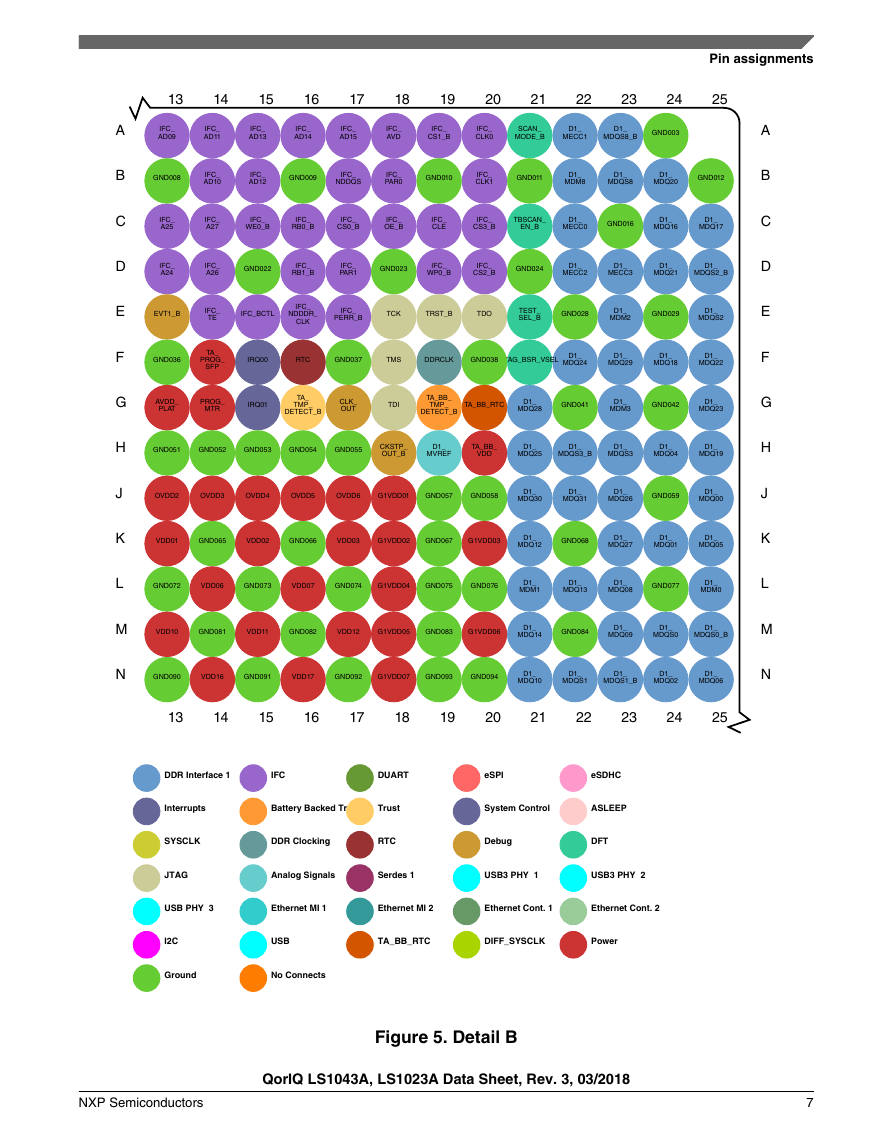
Pin assignments A B C D E F G H J K L M N A B C D E F G H J K L M N 13 14 15 16 17 18 19 20 21 22 23 24 25 IFC_ AD09 IFC_ AD11 IFC_ AD13 IFC_ AD14 IFC_ AD15 IFC_ AVD IFC_ CS1_B IFC_ CLK0 SCAN_ MODE_B D1_ MECC1 D1_ MDQS8_B GND003 GND008 IFC_ AD10 IFC_ AD12 GND009 IFC_ NDDQS IFC_ PAR0 GND010 IFC_ CLK1 GND011 D1_ MDM8 D1_ MDQS8 D1_ MDQ20 GND012 IFC_ A25 IFC_ A27 IFC_ WE0_B IFC_ RB0_B IFC_ CS0_B IFC_ OE_B IFC_ CLE IFC_ CS3_B TBSCAN_ EN_B D1_ MECC0 GND016 D1_ MDQ16 D1_ MDQ17 IFC_ A24 IFC_ A26 GND022 IFC_ RB1_B IFC_ PAR1 GND023 IFC_ WP0_B IFC_ CS2_B GND024 D1_ MECC2 D1_ MECC3 D1_ MDQ21 D1_ MDQS2_B EVT1_B IFC_ TE IFC_BCTL IFC_ NDDDR_ CLK IFC_ PERR_B TCK TRST_B TDO TEST_ SEL_B GND028 D1_ MDM2 GND029 D1_ MDQS2 GND036 TA_ PROG_ SFP IRQ00 RTC GND037 TMS DDRCLK GND038 JTAG_BSR_VSEL D1_ MDQ24 D1_ MDQ29 D1_ MDQ18 D1_ MDQ22 AVDD_ PLAT PROG_ MTR IRQ01 TA_ TMP_ DETECT_B CLK_ OUT TDI TA_BB_ TMP_ DETECT_B TA_BB_RTC D1_ MDQ28 GND041 D1_ MDM3 GND042 D1_ MDQ23 GND051 GND052 GND053 GND054 GND055 CKSTP_ OUT_B D1_ MVREF TA_BB_ VDD D1_ MDQ25 D1_ MDQS3_B D1_ MDQS3 D1_ MDQ04 D1_ MDQ19 OVDD2 OVDD3 OVDD4 OVDD5 OVDD6 G1VDD01 GND057 GND058 D1_ MDQ30 D1_ MDQ31 D1_ MDQ26 GND059 D1_ MDQ00 VDD01 GND065 VDD02 GND066 VDD03 G1VDD02 GND067 G1VDD03 D1_ MDQ12 GND068 D1_ MDQ27 D1_ MDQ01 D1_ MDQ05 GND072 VDD06 GND073 VDD07 GND074 G1VDD04 GND075 GND076 D1_ MDM1 D1_ MDQ13 D1_ MDQ08 GND077 D1_ MDM0 VDD10 GND081 VDD11 GND082 VDD12 G1VDD05 GND083 G1VDD06 D1_ MDQ14 GND084 D1_ MDQ09 D1_ MDQS0 D1_ MDQS0_B GND090 VDD16 GND091 VDD17 GND092 G1VDD07 GND093 GND094 D1_ MDQ10 D1_ MDQS1 D1_ MDQS1_B D1_ MDQ02 D1_ MDQ06 13 14 15 16 17 18 19 20 21 22 23 24 25 DDR Interface 1 IFC DUART eSPI eSDHC Interrupts Battery Backed Trust Trust System Control ASLEEP SYSCLK DDR Clocking RTC Debug DFT JTAG Analog Signals Serdes 1 USB3 PHY 1 USB3 PHY 2 USB PHY 3 Ethernet MI 1 Ethernet MI 2 Ethernet Cont. 1 Ethernet Cont. 2 I2C USB TA_BB_RTC DIFF_SYSCLK Power Ground No Connects Figure 5. Detail B NXP Semiconductors 7 QorIQ LS1043A, LS1023A Data Sheet, Rev. 3, 03/2018
Pin assignments N P R T U V W Y AA AB AC AD AE N P R T U V W Y AA AB AC AD AE 1 IIC1_ SCL 2 GND085 3 IIC4_ SDA 4 5 6 7 8 9 10 11 12 13 GND086 IRQ09 GND087 OVDD7 VDD13 GND088 VDD14 GND089 VDD15 GND090 SDHC_ DAT0 SDHC_ CMD SDHC_ CLK IRQ10 TH_ TPA TD1_ CATHODE GND095 GND096 VDD18 GND097 VDD19 GND098 VDD20 SDHC_ DAT2 SDHC_ DAT1 SPI_ CLK SPI_ MOSI SPI_ MISO TD1_ ANODE FA_ VL VDD23 GND104 VDD24 GND105 VDD25 GND106 SDHC_ DAT3 GND111 SPI_ CS0_B GND112 SPI_ CS1_B TH_ VDD ANALOG_ FA_ PIN GND113 VDD29 GND114 VDD30 GND115 VDD31 VDD32 GND119 VDD33 GND120 LVDD1 LVDD2 EC1_ RXD3 SPI_ CS3_B EC1_ GTX_ CLK SPI_ CS2_B GND118 ANALOG_ FA_ G_V EC1_ RX_ CLK EC1_ RXD2 GND122 EC1_ TXD3 EC1_ TXD2 IRQ11 TVDD SENSE GND GND123 GND124 GND125 GND126 GND127 GND128 EC1_ RXD1 EC1_ RXD0 EC1_ TXD1 GND131 EMI1_ MDIO EMI2_ MDIO SENSE VDD SD_ GND06 SD1_ REF_ CLK1_N SD1_ REF_ CLK1_P SD_ GND07 AVDD_ SD1_ PLL1 SD1_ IMP_ CAL_RX EC1_ RX_ DV EC2_ RX_ CLK GND133 EC1_ TXD0 EC2_ RXD3 EC1_ GTX_ CLK125 EC1_ TX_ EN EC2_ GTX_ CLK EC2_ RXD2 GND135 EC2_ TXD3 GND136 EC2_ RXD1 EC2_ RXD0 EC2_ TXD2 EC2_ TXD1 GND137 EC2_ RX_ DV GND139 EC2_ TXD0 EC2_ TX_ EN GND138 EC2_ GTX_ CLK125 1 2 3 4 EMI1_ MDC EMI2_ MDC NC_ Y7 SD_ GND08 SD_ GND09 SD_ GND10 SD_ GND11 SD_ GND12 NC_ Y13 NC_ AA5 NC_ AB5 NC_ AC5 NC_ AD5 NC_ AE5 5 NC_ AA6 NC_ AB6 NC_ AC6 NC_ AD6 NC_ AE6 6 NC_ AA7 NC_ AB7 NC_ AC7 NC_ AD7 NC_ AE7 7 NC_ AA8 NC_ AB8 NC_ AC8 NC_ AD8 NC_ AE8 8 NC_ AA9 NC_ AB9 NC_ AC9 NC_ AD9 NC_ AE9 9 NC_ AA10 NC_ AA11 NC_ AA12 SD_ GND18 NC_ AB10 NC_ AB11 NC_ AB12 SD_ GND21 NC_ AC10 NC_ AC11 NC_ AC12 SD_ GND24 NC_ AD10 NC_ AD11 NC_ AD12 SD_ GND32 NC_ AE10 NC_ AE11 NC_ AE12 SD_ GND36 10 11 12 13 DDR Interface 1 IFC DUART eSPI eSDHC Interrupts Battery Backed Trust Trust System Control ASLEEP SYSCLK DDR Clocking RTC Debug DFT JTAG Analog Signals Serdes 1 USB3 PHY 1 USB3 PHY 2 USB PHY 3 Ethernet MI 1 Ethernet MI 2 Ethernet Cont. 1 Ethernet Cont. 2 I2C USB TA_BB_RTC DIFF_SYSCLK Power Ground No Connects Figure 6. Detail C 8 NXP Semiconductors QorIQ LS1043A, LS1023A Data Sheet, Rev. 3, 03/2018
分享到:
收藏