ESMT
(Preliminary)
FM64D1G56A
1.8V NAND Flash + 1.8V Mobile DDR SDRAM Multi-Chip Package
Product Features
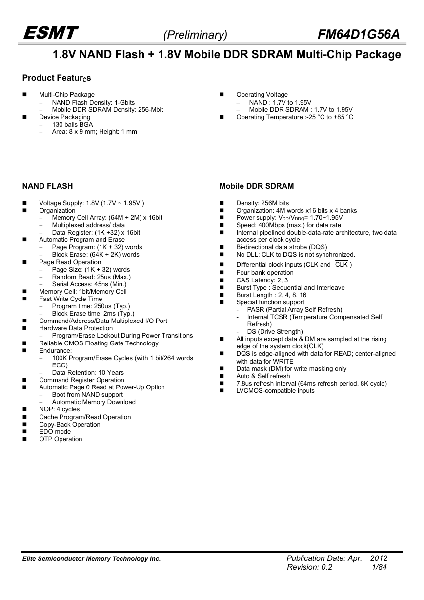
Multi-Chip Package
– NAND Flash Density: 1-Gbits
– Mobile DDR SDRAM Density: 256-Mbit
Device Packaging
–
130 balls BGA
– Area: 8 x 9 mm; Height: 1 mm
NAND FLASH
Voltage Supply: 1.8V (1.7V ~ 1.95V )
Organization
– Memory Cell Array: (64M + 2M) x 16bit
– Multiplexed address/ data
– Data Register: (1K +32) x 16bit
Automatic Program and Erase
– Page Program: (1K + 32) words
– Block Erase: (64K + 2K) words
Page Read Operation
– Page Size: (1K + 32) words
– Random Read: 25us (Max.)
– Serial Access: 45ns (Min.)
Memory Cell: 1bit/Memory Cell
Fast Write Cycle Time
– Program time: 250us (Typ.)
– Block Erase time: 2ms (Typ.)
Command/Address/Data Multiplexed I/O Port
Hardware Data Protection
– Program/Erase Lockout During Power Transitions
Reliable CMOS Floating Gate Technology
Endurance:
–
100K Program/Erase Cycles (with 1 bit/264 words
ECC)
– Data Retention: 10 Years
Command Register Operation
Automatic Page 0 Read at Power-Up Option
– Boot from NAND support
– Automatic Memory Download
NOP: 4 cycles
Cache Program/Read Operation
Copy-Back Operation
EDO mode
OTP Operation
Operating Voltage
– NAND : 1.7V to 1.95V
– Mobile DDR SDRAM : 1.7V to 1.95V
Operating Temperature :-25 °C to +85 °C
Mobile DDR SDRAM
Density: 256M bits
Organization: 4M words x16 bits x 4 banks
Power supply: VDD/VDDQ= 1.70~1.95V
Speed: 400Mbps (max.) for data rate
Internal pipelined double-data-rate architecture, two data
access per clock cycle
Bi-directional data strobe (DQS)
No DLL; CLK to DQS is not synchronized.
Differential clock inputs (CLK and CLK )
Four bank operation
CAS Latency: 2, 3
Burst Type : Sequential and Interleave
Burst Length : 2, 4, 8, 16
Special function support
- PASR (Partial Array Self Refresh)
-
Internal TCSR (Temperature Compensated Self
Refresh)
- DS (Drive Strength)
All inputs except data & DM are sampled at the rising
edge of the system clock(CLK)
DQS is edge-aligned with data for READ; center-aligned
with data for WRITE
Data mask (DM) for write masking only
Auto & Self refresh
7.8us refresh interval (64ms refresh period, 8K cycle)
LVCMOS-compatible inputs
Elite Semiconductor Memory Technology Inc.
Publication Date: Apr. 2012
1/84
Revision: 0.2
�
ESMT
Ordering Information
(Preliminary)
FM64D1G56A
Product ID
NAND Flash
Mobile DDR SDRAM
Configuration
Speed
Configuration
Speed
Package
Operation
Temperature
Range
FM64D1G56A -5BAGE
1Gb
(64M X 16 bits)
45ns
256Mb (4 Banks
X 4M X 16 bits)
200MHz
130 ball
BGA
Extended
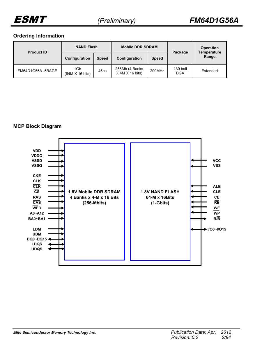
MCP Block Diagram
VDD
VDDQ
VSSD
VSSQ
CKE
CLK
CLK
CS
RAS
CAS
WED
A0~A12
BA0~BA1
1.8V Mobile DDR SDRAM
4 Banks x 4-M x 16 Bits
(256-Mbits)
DQ0~DQ15
LDM
UDM
LDQS
UDQS
1.8V NAND FLASH
64-M x 16Bits
(1-Gbits)
VCC
VSS
ALE
CLE
CE
RE
WE
WP
R/B
I/O0~I/O15
Elite Semiconductor Memory Technology Inc.
Publication Date: Apr. 2012
2/84
Revision: 0.2
�
ESMT
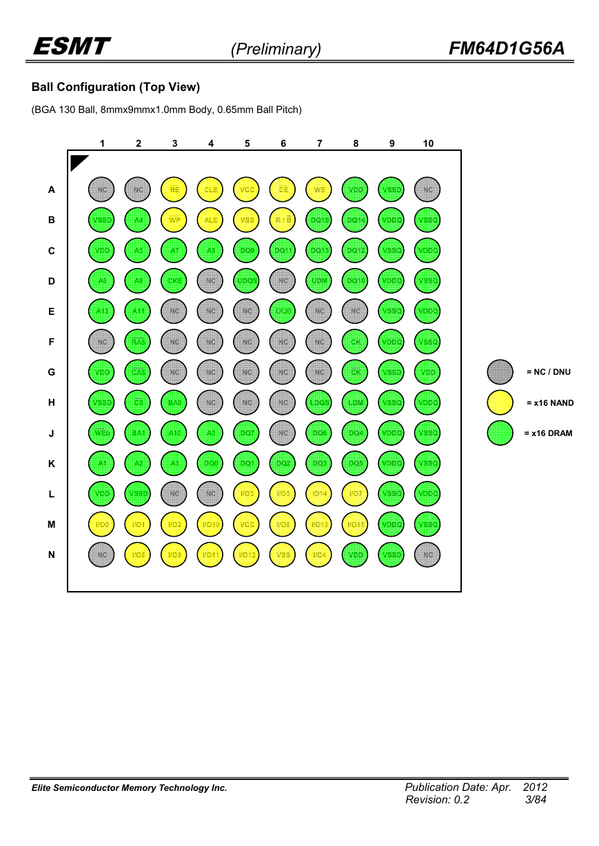
Ball Configuration (Top View)
(BGA 130 Ball, 8mmx9mmx1.0mm Body, 0.65mm Ball Pitch)
(Preliminary)
FM64D1G56A
1
2
3
4
5
6
7
8
9
10
NC
NC
RE
CLE
VCC
CE
WE
VDD
VSSD
NC
WP
ALE
VSS
R / B
DQ15
DQ14
VDDQ
VSSQ
A7
A9
DQ9
DQ11
DQ13
DQ12
VSSQ
VDDQ
CKE
NC
UDQS
NC
UDM
DQ10
VDDQ
VSSQ
VSSD
VDD
A6
A4
A5
A8
A12
A11
NC
RAS
VDD
CAS
VSSD
CS
BA0
WED
BA1
A10
A
B
C
D
E
F
G
H
J
K
L
M
N
NC
NC
NC
NC
NC
NC
NC
A0
NC
NC
NC
NC
DQ8
NC
NC
NC
NC
NC
NC
VSSQ
VDDQ
CK
VDDQ
VSSQ
CK
VSSD
VDD
NC
LDQS
LDM
VSSQ
VDDQ
DQ7
NC
DQ6
DQ4
VDDQ
VSSQ
= NC / DNU
= x16 NAND
= x16 DRAM
A1
A2
A3
DQ0
DQ1
DQ2
DQ3
DQ5
VDDQ
VSSQ
VDD
VSSD
NC
NC
I/O3
I/O5
ID14
I/O7
VSSQ
VDDQ
I/O0
I/O1
I/O2
I/O10
VCC
I/O6
I/O13
I/O15
VDDQ
VSSQ
NC
I/O8
I/O9
I/O11
I/O12
VSS
I/O4
VDD
VSSD
NC
Elite Semiconductor Memory Technology Inc.
Publication Date: Apr. 2012
3/84
Revision: 0.2
�
ESMT
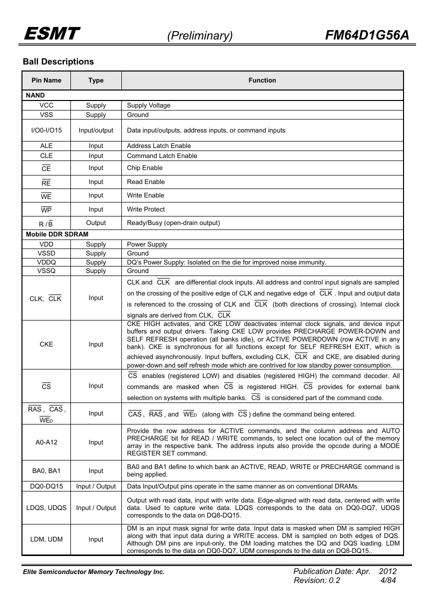
Ball Descriptions
(Preliminary)
FM64D1G56A
Pin Name
Type
Function
NAND
VCC
VSS
Supply
Supply
Supply Voltage
Ground
I/O0-I/O15
Input/output
Data input/outputs, address inputs, or command inputs
ALE
CLE
CE
RE
WE
WP
R / B
Input
Input
Input
Input
Input
Input
Output
Address Latch Enable
Command Latch Enable
Chip Enable
Read Enable
Write Enable
Write Protect
Ready/Busy (open-drain output)
Mobile DDR SDRAM
VDD
VSSD
VDDQ
VSSQ
Supply
Supply
Supply
Supply
CLK, CLK
Input
CKE
Input
CS
RAS , CAS ,
DWE
Input
Input
A0-A12
Input
Power Supply
Ground
DQ’s Power Supply: Isolated on the die for improved noise immunity.
Ground
CLK and CLK are differential clock inputs. All address and control input signals are sampled
on the crossing of the positive edge of CLK and negative edge of CLK . Input and output data
is referenced to the crossing of CLK and CLK (both directions of crossing). Internal clock
signals are derived from CLK, CLK
CKE HIGH activates, and CKE LOW deactivates internal clock signals, and device input
buffers and output drivers. Taking CKE LOW provides PRECHARGE POWER-DOWN and
SELF REFRESH operation (all banks idle), or ACTIVE POWERDOWN (row ACTIVE in any
bank). CKE is synchronous for all functions except for SELF REFRESH EXIT, which is
achieved asynchronously. Input buffers, excluding CLK, CLK and CKE, are disabled during
power-down and self refresh mode which are contrived for low standby power consumption.
CS enables (registered LOW) and disables (registered HIGH) the command decoder. All
commands are masked when CS is registered HIGH. CS provides for external bank
selection on systems with multiple banks. CS is considered part of the command code.
CAS , RAS , and
DWE (along with CS ) define the command being entered.
Provide the row address for ACTIVE commands, and the column address and AUTO
PRECHARGE bit for READ / WRITE commands, to select one location out of the memory
array in the respective bank. The address inputs also provide the opcode during a MODE
REGISTER SET command.
BA0, BA1
Input
BA0 and BA1 define to which bank an ACTIVE, READ, WRITE or PRECHARGE command is
being applied.
DQ0-DQ15
Input / Output Data Input/Output pins operate in the same manner as on conventional DRAMs.
LDQS, UDQS
Input / Output
LDM, UDM
Input
Output with read data, input with write data. Edge-aligned with read data, centered with write
data. Used to capture write data. LDQS corresponds to the data on DQ0-DQ7, UDQS
corresponds to the data on DQ8-DQ15.
DM is an input mask signal for write data. Input data is masked when DM is sampled HIGH
along with that input data during a WRITE access. DM is sampled on both edges of DQS.
Although DM pins are input-only, the DM loading matches the DQ and DQS loading. LDM
corresponds to the data on DQ0-DQ7, UDM corresponds to the data on DQ8-DQ15..
Elite Semiconductor Memory Technology Inc.
Publication Date: Apr. 2012
4/84
Revision: 0.2
�
ESMT
PACKING
130-BALL
DIMENSIONS
( 8x9 mm )
D
PIN #1
"A"
e
D1
PIN #1
"B"
Symbol
A
A1
Φb
D
E
D1
E1
e
ccc
Min
0.16
0.25
7.90
8.90
Dimension in mm
Norm
0.21
0.30
8.00
9.00
5.85 BSC
7.80 BSC
0.65 BSC
Controlling dimension : Millimeter.
(Preliminary)
FM64D1G56A
E
C
A
1
A
ccc C
SEATING PLANE
DETAIL : "A"
SOLDER BALL
1
E
DETAIL : "B"
Max
1.00
0.27
0.35
8.10
9.10
Min
0.006
0.010
0.311
0.350
0.10
Dimension in inch
Norm
0.008
0.012
0.315
0.354
0.230 BSC
0.307 BSC
0.026 BSC
Max
0.039
0.011
0.014
0.319
0.358
0.004
Elite Semiconductor Memory Technology Inc.
Publication Date: Apr. 2012
5/84
Revision: 0.2
�
ESMT
(Preliminary)
FM64D1G56A
NAND Flash Memory Operations
Elite Semiconductor Memory Technology Inc.
Publication Date: Apr. 2012
6/84
Revision: 0.2
�
(Preliminary)
FM64D1G56A
inputs as well as data input/output. The copy back function
allows the optimization of defective blocks management: when
a page program operation fails the data can be directly
programmed in another page inside the same array section
without the time consuming serial data insertion phase. The
cache program feature allows the data insertion in the cache
register while the data register is copied into the Flash array.
This pipelined program operation
the program
throughput when long files are written inside the memory. A
cache read feature is also implemented. This feature allows to
dramatically improving the read throughput when consecutive
pages have to be streamed out. This NAND Flash includes
extra feature: Automatic Read at Power Up.
improves
ESMT
GENERAL DESCRIPTION
The NAND Flash is a 64Mx16bit with spare 2Mx16bit capacity.
The NAND Flash is offered in 1.8V VCC Power Supply. Its NAND
cell provides the most cost-effective solution for the solid state
mass storage market. The memory is divided into blocks that
can be erased independently so it is possible to preserve valid
data while old data is erased.
The NAND Flash contains 1,024 blocks, composed by 64 pages
consisting in two NAND structures of 32 series connected Flash
cells. A program operation allows to write the 1,056-word page
in typical 250us and an erase operation can be performed in
typical 2ms on a 64K-word for device block.
Data in the page mode can be read out at 45ns cycle time per
Byte. The I/O pins serve as the ports for address and command
PIN DESCRIPTION
Symbol
Pin Name
Functions
I/O0~ I/O15 Data Inputs / Outputs
CLE
Command Latch Enable
ALE
Address Latch Enable
The I/O pins are used to input command, address and data, and to output data
during read operations. The I/O pins float to Hi-Z when the chip is deselected or
when the outputs are disabled.
The CLE input controls the activating path for commands sent to the command
register. When active high, commands are latched into the command register
through the I/O ports on the rising edge of the WE signal.
The ALE input controls the activating path for address to the internal address
registers. Addresses are latched on the rising edge of WE with ALE high.
CE
Chip Enable
The CE input is the device selection control. When the device is in the Busy
state, CE high is ignored, and the device does not return to standby mode.
RE
Read Enable
WE
Write Enable
WP
Write Protect
R / B
Ready / Busy Output
The RE input is the serial data-out control, and when active drives the data onto
the I/O bus. Data is valid tREA after the falling edge of RE which also increments
the internal column address counter by one.
The WE input controls writes to the I/O port. Commands, address and data are
latched on the rising edge of the WE pulse.
The WP pin provides inadvertent program/erase protection during power
transitions. The internal high voltage generator is reset when the WP pin is
active low.
The R/ B output indicates the status of the device operation. When low, it
indicates that a program, erase or random read operation is in process and returns
to high state upon completion. It is an open drain output and does not float to Hi-Z
condition when the chip is deselected or when outputs are disabled.
Power
Ground
VCC
VSS
VCC is the power supply for device.
Note: Connect all VCC and VSS pins of each device to common power supply outputs. Do not leave VCC or VSS disconnected.
Elite Semiconductor Memory Technology Inc.
Publication Date: Apr. 2012
7/84
Revision: 0.2
�
ESMT
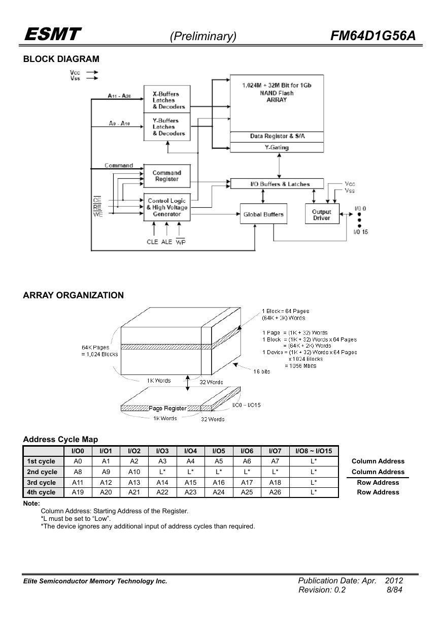
BLOCK DIAGRAM
(Preliminary)
FM64D1G56A
ARRAY ORGANIZATION
Address Cycle Map
I/O0
A0
A8
A11
A19
I/O1
A1
A9
A12
A20
I/O2
A2
A10
A13
A21
I/O3
A3
L*
A14
A22
I/O4
A4
L*
A15
A23
I/O5
A5
L*
A16
A24
I/O6
A6
L*
A17
A25
I/O7
A7
L*
A18
A26
I/O8 ~ I/O15
L*
L*
L*
L*
Column Address
Column Address
Row Address
Row Address
1st cycle
2nd cycle
3rd cycle
4th cycle
Note:
Column Address: Starting Address of the Register.
*L must be set to “Low”.
*The device ignores any additional input of address cycles than required.
Elite Semiconductor Memory Technology Inc.
Publication Date: Apr. 2012
8/84
Revision: 0.2
�




 2023年江西萍乡中考道德与法治真题及答案.doc
 2012年重庆南川中考生物真题及答案.doc
 2013年江西师范大学地理学综合及文艺理论基础考研真题.doc
 2020年四川甘孜小升初语文真题及答案I卷.doc
 2020年注册岩土工程师专业基础考试真题及答案.doc
 2023-2024学年福建省厦门市九年级上学期数学月考试题及答案.doc
 2021-2022学年辽宁省沈阳市大东区九年级上学期语文期末试题及答案.doc
 2022-2023学年北京东城区初三第一学期物理期末试卷及答案.doc
 2018上半年江西教师资格初中地理学科知识与教学能力真题及答案.doc
 2012年河北国家公务员申论考试真题及答案-省级.doc
 2020-2021学年江苏省扬州市江都区邵樊片九年级上学期数学第一次质量检测试题及答案.doc
 2022下半年黑龙江教师资格证中学综合素质真题及答案.doc