Op Amp Rectifiers, Peak Detectors and Clamps
AN1353
Author:
Dragos Ducu,
Microchip Technology Inc.
INTRODUCTION
This application note covers a wide range of
applications, such as half-wave rectifiers, full-wave
rectifiers, peak detectors and clamps. Many of the
circuits are simple in terms of component count, but
they play important roles in overall systems design,
such as:
• AC to DC Power Conversion
• Automatic Gain Control Loops
• Power Monitoring Applications
• AM Demodulator
BASIC RECTIFIERS
The basic rectifiers have been designed with diodes.
Figure 1 shows such a simple series circuit, driven by
an AC source. When the diode is reverse-biased, it
acts as a very high impedance device. Figure 1shows
a negative half wave rectifier. It outputs nearly the full
input voltage across the diode when reverse biased. A
similar circuit in Figure 2 shows a positive half-wave
rectifier. If a full-wave rectifier is desired, more diodes
must be used to configure a bridge, as shown in
Figure 3. The input signal must be larger than the
voltage across the diode to ensure that the diode is
forward biased.
AC
D1
VOUT
V
RL
t
VIN
VOUT
FIGURE 1:
Rectifier.
Negative Half-Wave
AC
D1
VOUT
V
RL
t
VIN
VOUT
FIGURE 2:
Positive Half-Wave Rectifier.
V
VOUT
RL
t
VIN
VOUT
FIGURE 3:
Full-Wave Rectifier.
Choosing the Components
the diode,
SELECTING THE DIODE
When choosing
important
parameters are the maximum forward current (IF), and
the peak inverse voltage rating (PIV) of the diode. The
peak inverse voltage is the maximum voltage the diode
can withstand when it is reverse-biased. If this voltage
is exceeded, the diode may be destroyed. The diode
must have a peak inverse voltage rating that is higher
than the maximum voltage applied
in an
application. In many diode data sheets, PIV is referred
to as peak reverse voltage (PRV).
the most
to it
© 2011 Microchip Technology Inc.
DS01353A-page 1
�
AN1353
The peak inverse voltage of the diode will be equal to:
TABLE 1:
EQUATION 1:
VPIV rating
(
) VPK max
≥
(
) VD on(
+
)
Where:
VPIV = Peak inverse voltage
VPK(max) = Maximum peak amplitude
VD(on) = Diode voltage on when in
leading
is nonlinear,
Every diode has a parasitic capacitance and, by
default, has a time charge storage. This charge storage
mechanism
to a nonlinear
capacitance. This effect is very important because the
nonlinearity of the diode can generate harmonics. For
example, the output voltage becomes negative for a
short time. This period is called reverse recovery time.
During the transition, the diode’s parasitic capacitance
will interact with the circuit resistors to modify the
circuit’s behavior.
For most general purpose applications, low power
signal diodes such as 1N4148, are adequate. For high
accuracy applications, where offset errors and reverse
diode leakage current are critical, a low leakage FET
transistor can be used as a diode (short Drain and
Source together), such as 2N4117A. In applications
where speed is important, silicon Schottky barrier
diodes are worth considering, since they have a low
forward ON voltage of only 0.4V and are fast.
SELECTING THE RESISTOR
The resistor is selected based on the load current.
One limitation is the value of load resistor. The value of
the load resistor must be less than the diode resistance
when in reverse bias. The parasitic capacitance of the
diode interacts with the load resistor causing a time
constant. If this constant is large, the output voltage will
have a delayed recovery.
Advantages and Disadvantages
The major disadvantage of these circuits is the
nonlinearity of the diodes. If the input signal is smaller
than the threshold voltage of the diode, the signal
cannot be recovered. To reduce the threshold voltage
of the diode and improve linearity, we need to include
the diode into the feedback loop of the operational
amplifier.
Practical Examples
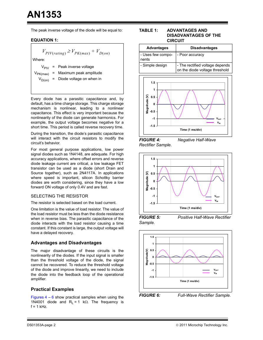
Figures 4 – 6 show practical samples when using the
1N4001 diode and RL = 1 kΩ. The frequency is
f = 1 kHz.
ADVANTAGES AND
DISADVANTAGES OF THE
CIRCUIT
Advantages
- Uses few compo-
nents
- Simple design
Disadvantages
- Poor accuracy
- The rectified voltage depends
on the diode voltage threshold
)
V
(
e
d
u
t
i
n
g
a
M
1.5
1
0.5
0
-0.5
-1
-1.5
FIGURE 4:
Rectifier Sample.
)
V
(
e
d
u
t
i
n
g
a
M
1.5
1
0.5
0
-0.5
-1
-1.5
FIGURE 5:
Sample.
)
V
(
e
d
u
t
i
n
g
a
M
1.5
1
0.5
0
-0.5
-1
-1.5
VOUT
VIN
Time (1 ms/div)
Negative Half-Wave
VOUT
VIN
Time (1 ms/div)
Positive Half-Wave Rectifier
VOUT
VIN
Time (1 ms/div)
FIGURE 6:
Full-Wave Rectifier Sample.
DS01353A-page 2
© 2011 Microchip Technology Inc.
�
ACTIVE HALF-WAVE RECTIFIER
The simplest op amp half-wave rectifier is shown in
Figure 7. When the VIN is positive, the diode is forward
biased; the signal can be found on the RL load. When
the VIN is negative, the diode is non-conductive, and
the output signal is ground (0V).
VIN
-
+
AO1
D1
VOUT
RL
FIGURE 7:
Op Amp Half-Wave Rectifier.
The big advantage of this circuit is represented by the
small threshold voltage and linearity. This is more
convenient than the basic rectifiers, since this circuit is
able to rectify signals smaller than the diode threshold
voltage.
)
V
(
e
d
u
t
i
n
g
a
M
1.50
1.00
0.50
0.00
-0.50
-1.00
-1.50
AN1353
Choosing the Components
SELECTING THE OP AMP
When selecting
the op amp,
characteristics must be considered:
• Gain Bandwidth Product
• Slew Rate (SR)
The minimum gain bandwidth product requirement can
be estimated in Equation 2.
important
two
EQUATION 2:
fGBWP
=
10 G× fINPUT
×
Where:
fGBWP = Gain bandwidth product
G = DC gain
fINPUT = Maximum input frequency
The next parameter that needs to be considered is the
slew rate (SR). This is the maximum time rate change
at the output of the op amp; it shows how fast the output
can follow the input signal. The SR parameter can be
found in the selected op amp’s data sheet.
The full bandwidth product (FPBW) defines the highest
frequency sine wave that will not be distorted by the
slew rate limit.
VOUT
VIN
EQUATION 3:
Time (1 ms/div)
Circuit Behavior on
FIGURE 8:
Low Frequency.
This circuit has limitations. The rectifier’s speed is
limited by the op amp bandwidth. This effect is
illustrated in Figure 9, where the rectified output signal
overlaps the input signal. The maximum frequency
that can be rectified is determined by the slew rate of
the op amp.
VOUT
VIN
)
V
(
e
d
u
t
i
n
g
a
M
1.5
1
0.5
0
-0.5
-1
-1.5
FIGURE 9:
High-Frequency Input Signals.
Time (50 µs/div)
Output Limitation on
=
SR ΔVOUT
-----------------
ΔT
max
SR
FPBW
=
-------------------------------------
π VOUT p
×
p–(
)
SELECTING THE DIODE AND THE RESISTOR
Refer to the sections Selecting the Diode and Selecting
The Resistor, in the Basic Rectifiers section, for details
on choosing the appropriate components.
Advantages and Disadvantages
Table 2
disadvantages of a half-wave rectifier.
TABLE 2:
the main
shows
ADVANTAGES AND
DISADVANTAGES OF THE
CIRCUIT
advantages
and
Advantages
Disadvantages
- Uses few components - Load dependant
- Good linearity
- Limited op amp bandwidth
© 2011 Microchip Technology Inc.
DS01353A-page 3
�
AN1353
Practical Example
This example of a half-wave rectifier uses an
MBRM110LT3 Schottky diode and the MCP661 op
amp with different load resistors. For this example, the
value of the load resistor is less than 1 kΩ, to avoid
glitches in the negative cycle. The Schottky diode is
chosen for higher speed than a small signal silicon
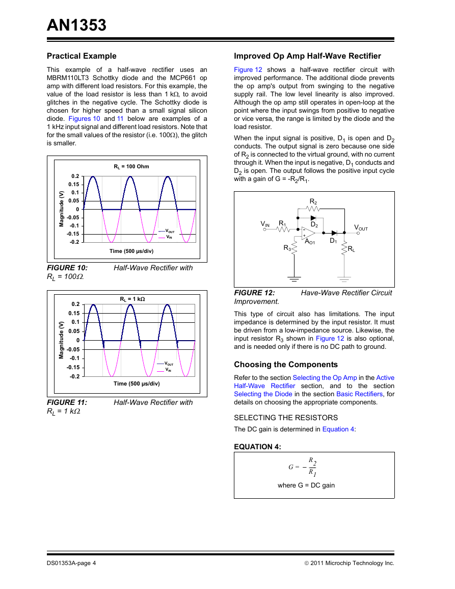
diode. Figures 10 and 11 below are examples of a
1 kHz input signal and different load resistors. Note that
for the small values of the resistor (i.e. 100Ω), the glitch
is smaller.
RL = 100 Ohm
)
V
(
e
d
u
t
i
n
g
a
M
0.2
0.15
0.1
0.05
0
-0.05
-0.1
-0.15
-0.2
FIGURE 10:
RL = 100Ω.
)
V
(
e
d
u
t
i
n
g
a
M
0.2
0.15
0.1
0.05
0
-0.05
-0.1
-0.15
-0.2
FIGURE 11:
RL = 1 kΩ.
VOUT
VIN
Time (500 µs/div)
Half-Wave Rectifier with
RL = 1 k:
��������VOUT
VIN
Time (500 µs/div)
Half-Wave Rectifier with
Improved Op Amp Half-Wave Rectifier
Figure 12 shows a half-wave rectifier circuit with
improved performance. The additional diode prevents
the op amp's output from swinging to the negative
supply rail. The low level linearity is also improved.
Although the op amp still operates in open-loop at the
point where the input swings from positive to negative
or vice versa, the range is limited by the diode and the
load resistor.
When the input signal is positive, D1 is open and D2
conducts. The output signal is zero because one side
of R2 is connected to the virtual ground, with no current
through it. When the input is negative, D1 conducts and
D2 is open. The output follows the positive input cycle
with a gain of G = -R2/R1.
R2
D2
-
+
AO1
VIN R1
R3
VOUT
D1
RL
Have-Wave Rectifier Circuit
FIGURE 12:
Improvement.
This type of circuit also has limitations. The input
impedance is determined by the input resistor. It must
be driven from a low-impedance source. Likewise, the
input resistor R3 shown in Figure 12 is also optional,
and is needed only if there is no DC path to ground.
Choosing the Components
Refer to the section Selecting the Op Amp in the Active
Half-Wave Rectifier section, and
the section
Selecting the Diode in the section Basic Rectifiers, for
details on choosing the appropriate components.
to
SELECTING THE RESISTORS
The DC gain is determined in Equation 4:
EQUATION 4:
G = –
R2
------
R1
where G = DC gain
DS01353A-page 4
© 2011 Microchip Technology Inc.
�
AN1353
For an input frequency under 600 kHz, the circuit
performs properly. For frequencies larger than this
value, the output signal is distorted.
)
V
(
e
d
u
t
i
n
g
a
M
1
0.8
0.6
0.4
0.2
0
-0.2
-0.4
-0.6
-0.8
-1
VOUT
VIN
Time (0.2 µs/div)
Circuit Behavior with
FIGURE 14:
600 kHz Input Frequency.
To design a negative half-wave rectifier using the same
components, we only have to invert the diodes, as
shown in the circuit in Figure 15.
and
R2
D2
-
+
AO1
VIN
R1
R3
D1
VOUT
RL
FIGURE 15:
Rectifier.
Negative Half-Wave
VOUT
VIN
)
V
(
e
d
u
t
i
n
g
a
M
0.2
0.15
0.1
0.05
0
-0.05
-0.1
-0.15
-0.2
Resistors R1 and R2 are selected based on the
application design:
• For a general purpose application, the resistor’s
value should be between 1 kΩ and 100 kΩ.
• For a high speed application, the resistor’s value
should be between 100 Ω and 1 kΩ (consume
more power)
• For portable applications between 1 MΩ and
10 MΩ.
The R3 is added to minimize the error caused by the
input bias current.
EQUATION 5:
=
R3
R1 R2×
R1 R2+--------------------
Advantages and Disadvantages
Table 3
advantages
disadvantages of an improved half-wave rectifier.
TABLE 3:
the main
shows
ADVANTAGES AND
DISADVANTAGES OF THE
CIRCUIT
Advantages
Disadvantages
- Uses more components
- Low impedance
because of R1
- Good linearity
- The second diode
prevents the op amp from
swinging into the negative
cycle
Practical Example
The example in Figure 13 is based on the circuit in
Figure 12, and uses the MCP661 op amp, two
MBRM110LT3 Schottky diodes, RL = 1 kΩ, R2 =10 kΩ
and R1 = 1 kΩ. The input frequency is 1 kHz.
RL = 1 k:
)
V
(
e
d
u
t
i
n
g
a
M
0.2
0.15
0.1
0.05
0
-0.05
-0.1
-0.15
-0.2
VOUT
VIN
Time (1 ms/div)
Time (1 ms/div)
Negative Cycle Rectifier
FIGURE 16:
Sample.
FIGURE 13:
Rectifier with RL = 1 KΩ.
Improved Half-Wave
© 2011 Microchip Technology Inc.
DS01353A-page 5
�
AN1353
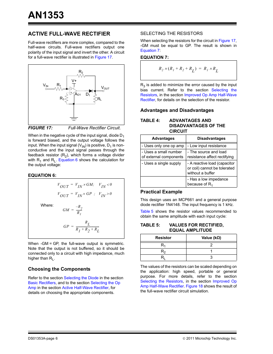
ACTIVE FULL-WAVE RECTIFIER
Full-wave rectifiers are more complex, compared to the
half-wave circuits. Full-wave rectifiers output one
polarity of the input signal and invert the other. A circuit
for a full-wave rectifier is illustrated in Figure 17.
SELECTING THE RESISTORS
When selecting the resistors for the circuit in Figure 17,
-GM must be equal to GP. The result is shown in
Equation 7:
EQUATION 7:
R2
V+
-
+
AO1
VOUT
D1
RL
VIN
R1
R3
Full-Wave Rectifier Circuit.
FIGURE 17:
When in the negative cycle of the input signal, diode D1
is forward biased, and the output voltage follows the
input. When the input signal (VIN) is positive, D1 is non-
conductive and the input signal passes through the
feedback resistor (R2), which forms a voltage divider
with R1 and RL. Equation 6 shows the calculation for
the output voltage:
EQUATION 6:
VOUT
VOUT
=
=
VIN GM×
VIN GP×
;
;
VIN 0<
VIN 0>
Where:
GM
=
R2–
---------
R1
GP
=
RL
+
-----------------------------------
R1 R2 RL
+
When -GM = GP, the full-wave output is symmetric.
Note that the output is not buffered, so it should be
connected only to a circuit with high impedance, much
higher than RL.
Choosing the Components
Refer to the section Selecting the Diode in the section
Basic Rectifiers, and to the section Selecting the Op
Amp in the section Active Half-Wave Rectifier, for
details on choosing the appropriate components.
R2
(
×
+
R1 R2 RL
+
)
R1 RL×=
R3 is added to minimize the error caused by the input
bias current. Refer to the section Selecting the
Resistors, in the section Improved Op Amp Half-Wave
Rectifier, for details on the selection of the resistor.
Advantages and Disadvantages
TABLE 4:
ADVANTAGES AND
DISADVANTAGES OF THE
CIRCUIT
Advantages
Disadvantages
- Uses only one op amp - Low input resistance
- The source and load
- Uses a small number
resistance affect rectifying
of external components
- A reactive load (capacitor
- Uses a single supply
or coil) cannot be tolerated
without a buffer
- Has a low impedance
because of R1
Practical Example
This design uses an MCP661 and a general purpose
diode rectifier 1N4148. The input frequency is 1 kHz.
Table 5 shows the resistor values recommended to
obtain the same amplitude with each input cycle:
VALUES FOR RECTIFIED,
TABLE 5:
EQUAL AMPLITUDE
Resistor
Value (kΩ)
R1
R2
RL
2
1
3
The values of the resistors can be scaled depending on
the application: high speed, portable or general
purpose. For more details, refer to the section
Selecting the Resistors, in the section Improved Op
Amp Half-Wave Rectifier. Figure 18 shows the result of
the full-wave rectifier circuit simulation.
DS01353A-page 6
© 2011 Microchip Technology Inc.
�
AN1353
EQUATION 8:
=
VO1
VIN G when
,×
VIN > 0
Where:
G
=
R1–
---------
R2
VO1
,=
0 when VIN 0<
Equation 9 calculates the output voltage:
EQUATION 9:
VOUT
=
–
R5 VO1×
------------------------
R3
–
R5 V× IN
-----------------------
R4
Choosing the Components
To obtain a good performance for the two stage circuit,
the tolerance of resistors R1 to R5 should be 1%, or
better; this makes the gains (for negative and positive
VIN) match well. The circuit in Figure 19 has a good
linearity, down to a couple of mV at low frequencies, but
the high-frequency response is limited by the op amp
bandwidth.
Refer to the section Selecting the Diode in the section
Basic Rectifiers, and to the section Selecting the Op
Amp in the section Active Half-Wave Rectifier, for
details on choosing the appropriate components.
SELECTING THE RESISTORS
R1 and R2 give the gain for the first stage; R3 and R5
for the second stage.
To get the same amplitude for both cycles, choose
R1 = R3 = R4 and R2 = R5 = 2 x R1.
EQUATION 10:
VOUT
–=
×
(
R5
VO1 VIN+
)
----------------------------------------------
R1
R6 is added to minimize the error caused by the input
bias current. Refer to the section Selecting the
Resistors, in the section Improved Op Amp Half-Wave
Rectifier, for details on choosing the appropriate
components.
If a greater sensitivity and high frequency is desired, it
is recommended to use lower resistance value, high
speed diodes and faster op amps.
)
V
(
e
d
u
t
i
n
g
a
M
0.2
0.15
0.1
0.05
0
-0.05
-0.1
-0.15
-0.2
VOUT
VIN
Time (1ms/div)
FIGURE 18:
Simulation with the Recommended Values of the
Resistors.
Full-Wave Rectifier Circuit
TWO STAGE OP AMP FULL-WAVE
RECTIFIER
Another full-wave rectifier can be obtained by including
an adder to the single-wave rectifier, which subtracts
VIN from the rectified signal. The rectifier stage consists
of AO1, R1, R2, D1 and D2, while the adder stage
consists of AO2, R3, R4 and R5.
VIN
R1
R2
D2
-
+
AO1
D1
R3
R5
VO1
R4
R6
VOUT
-
+
AO2
Two Stage Op Amp Full-
FIGURE 19:
Wave Rectifier Circuit.
When VIN is positive, D1 is forward-biased and D2 is
reverse-biased, while when VIN is negative, D2 is
forward-biased and D1 is reversed-biased. The second
stage adds VIN and VO1 and inverts the polarity of the
resulting signal. The output voltage for the positive
cycle of the input voltage is calculated in Equation 8.
For the negative cycle of the input voltage (VIN), D1
blocks the signal, while D2 conducts the whole current
coming from the input. In this case, the output voltage
for the first stage is VO1 = 0V.
For the positive cycle of the input signal, VO1 is
negative and, in this case, the adder stage combines
the input signals with equal amplitudes, one positive
and one negative.
© 2011 Microchip Technology Inc.
DS01353A-page 7
�
AN1353
Advantages and Disadvantages
Table 6 shows the advantages and disadvantages of a
two stage op amp full-wave rectifier.
TABLE 6:
ADVANTAGES AND
DISADVANTAGES OF THE
CIRCUIT
Advantages
Disadvantages
- Very good performance - Uses two op amps
- Low output impedance - Low input resistance
- Multiple passive
components
Practical Example
This example uses the MCP6021 device, two 1N4148
diodes, R1 = 1 kΩ, R2 = 2 kΩ, R3 = 1 kΩ, R4 = 1 kΩ,
and R5 = 2 kΩ. The input signal frequency is f = 1 kHz.
Figure 20 shows the result of the simulation for the full-
wave rectifier shown in Figure 19:
)
V
(
e
d
u
t
i
n
g
a
M
1
0.8
0.6
0.4
0.2
0
-0.2
-0.4
-0.6
-0.8
-1
VOUT
VIN
Time (1 ms/div)
Full-Wave Rectifier Circuit
FIGURE 20:
Simulation.
For more topologies of the full-wave rectifier, refer to
the Appendix section.
Figure 21 shows the behavior of the circuit at the
maximum frequency tolerated.
)
V
(
e
d
u
t
i
n
g
a
M
1
0.8
0.6
0.4
0.2
0
-0.2
-0.4
-0.6
-0.8
-1
VOUT
VIN
Time (10 µs/div)
FIGURE 21:
Frequency = 100 kHz.
Circuit Behavior when Input
BASIC PEAK DETECTORS
The purpose of this circuit is to detect the maximum
magnitude of a signal over a period of time. The
operation of a peak detector can be illustrated using a
simple diode and capacitor, as shown in Figure 22.
VIN
D1
C1
VOUT
R1
FIGURE 22:
Operation.
Basic Peak Detector
Choosing the Components
When choosing the resistor, the limits must be
considered: rdf << R1 << rdr, where rdf is the resistance
of the diode when forward biased, and rdr is the
resistance of the diode when reverse biased.
The capacitor is charged with the time constant
τ1 = rdf x C1, and will be discharged with the time
constant τ2=R1 x C1.
The variation of output voltage will be:
EQUATION 11:
ΔV
=
Where:
VPEAK
-------------------
f τ2×
VPEAK = Amplitude maximum value
f = Input signal frequency
τ2 = Discharge time constant
Generally the minimum of τ2 is τ2 = 10/f.
This is the case for a sine signal, but we may need to
detect the peak for other types of signals, such as
square waves, sensors or modulated signals.
For example, on an amplitude modulated signal, the
capacitor voltage discharges according to:
EQUATION 12:
=
VDROP
exp×
Where: τ2 = time constant
VPEAK
t
⎛
⎞
-----–⎝
⎠
τ2
This produces a negative peak clipping that distorts the
output. To avoid the negative peak clipping, choose a
smaller value for τ2, but to reduce the ripple, τ2 must be
as large as possible. In practice we choose a value
between: 1/fm >> τ2 >> 1/fc, where fm is the modulation
frequency and fc is the carrier frequency.
DS01353A-page 8
© 2011 Microchip Technology Inc.
�





 2023年江西萍乡中考道德与法治真题及答案.doc
 2012年重庆南川中考生物真题及答案.doc
 2013年江西师范大学地理学综合及文艺理论基础考研真题.doc
 2020年四川甘孜小升初语文真题及答案I卷.doc
 2020年注册岩土工程师专业基础考试真题及答案.doc
 2023-2024学年福建省厦门市九年级上学期数学月考试题及答案.doc
 2021-2022学年辽宁省沈阳市大东区九年级上学期语文期末试题及答案.doc
 2022-2023学年北京东城区初三第一学期物理期末试卷及答案.doc
 2018上半年江西教师资格初中地理学科知识与教学能力真题及答案.doc
 2012年河北国家公务员申论考试真题及答案-省级.doc
 2020-2021学年江苏省扬州市江都区邵樊片九年级上学期数学第一次质量检测试题及答案.doc
 2022下半年黑龙江教师资格证中学综合素质真题及答案.doc