MALD-37030B
26 Gbps Multi-Rate Laser Driver with Limiting Amplifier, Dual CDRs,
Power Management, and Diagnostics
Features
• DC coupled laser driver with up to 100mA bias and 76mA modulation current
•
Internal buck-boost converter for automatic laser anode voltage optimization
• Reference-free TX and RX CDRs with bypass and multi-rate re-timing
Applications
• SFP28 Optical Modules
• Active Optical Cables
• 25-Gigabit Ethernet 25GbE
• CPRI
• SFP28
• 25G & 21G VCO, half rate re-timing (MALD-37030)
• High input jitter tolerance with low output jitter
•
Internal or external temperature sensor, supply voltage monitor, TX power
monitor, RSSI indicator
Integrated PRBS generator and checker and bidirectional loop back
Integrated Fibre Channel RS0/RS1 rate select functionality
• Programmable AC or DC LOS threshold and slice level adjust on RX channel
•
•
• Powered from a single 3.3V with internal 1.8V buck converter
• Supports -40 °C to +95 °C temperature range
Rev V2
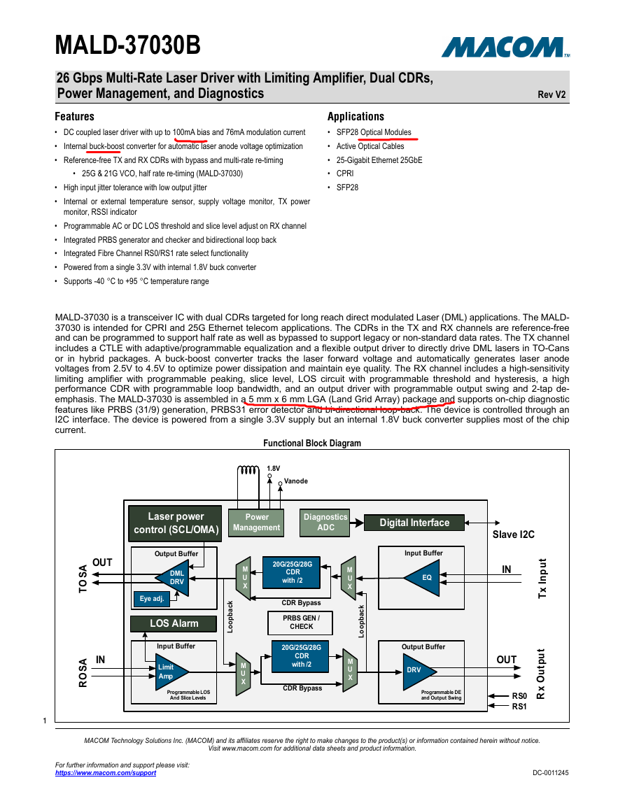
MALD-37030 is a transceiver IC with dual CDRs targeted for long reach direct modulated Laser (DML) applications. The MALD-
37030 is intended for CPRI and 25G Ethernet telecom applications. The CDRs in the TX and RX channels are reference-free
and can be programmed to support half rate as well as bypassed to support legacy or non-standard data rates. The TX channel
includes a CTLE with adaptive/programmable equalization and a flexible output driver to directly drive DML lasers in TO-Cans
or in hybrid packages. A buck-boost converter tracks the laser forward voltage and automatically generates laser anode
voltages from 2.5V to 4.5V to optimize power dissipation and maintain eye quality. The RX channel includes a high-sensitivity
limiting amplifier with programmable peaking, slice level, LOS circuit with programmable threshold and hysteresis, a high
performance CDR with programmable loop bandwidth, and an output driver with programmable output swing and 2-tap de-
emphasis. The MALD-37030 is assembled in a 5 mm x 6 mm LGA (Land Grid Array) package and supports on-chip diagnostic
features like PRBS (31/9) generation, PRBS31 error detector and bi-directional loop-back. The device is controlled through an
I2C interface. The device is powered from a single 3.3V supply but an internal 1.8V buck converter supplies most of the chip
current.
Functional Block Diagram
1.8V
Vanode
Laser power
control (SCL/OMA)
Power
Management
Diagnostics
ADC
Digital Interface
Slave I2C
OUT
A
S
O
T
IN
A
S
O
R
Output Buffer
DML
DRV
Eye adj.
LOS Alarm
Input Buffer
Limit
Amp
Programmable LOS
And Slice Levels
k
c
a
b
p
o
o
L
M
U
X
M
U
X
20G/25G/28G
CDR
with /2
CDR Bypass
PRBS GEN /
CHECK
20G/25G/28G
CDR
with /2
CDR Bypass
M
U
X
M
U
X
k
c
a
b
p
o
o
L
Input Buffer
EQ
IN
Output Buffer
DRV
Programmable DE
and Output Swing
OUT
RS0
RS1
t
u
p
n
I
x
T
t
u
p
t
u
O
x
R
1
MACOM Technology Solutions Inc. (MACOM) and its affiliates reserve the right to make changes to the product(s) or information contained herein without notice.
Visit www.macom.com for additional data sheets and product information.
For further information and support please visit:
https://www.macom.com/support
DC-0011245
�
MALD-37030B
26 Gbps Multi-Rate Laser Driver with Limiting Amplifier, Dual CDRs,
Power Management, and Diagnostics
Rev V2
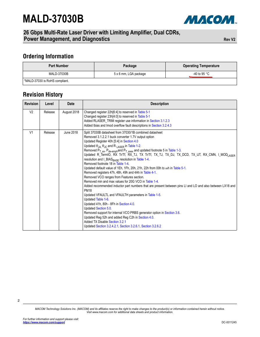
Ordering Information
Part Number
MALD-37030B
*MALD-37030 is RoHS compliant.
Revision History
Revision
Level
Date
V2
Release
August 2018
V1
Release
June 2018
Package
5 x 6 mm, LGA package
Operating Temperature
-40 to 95 °C
Description
Changed register 22h[6:4] to reserved in Table 5-1
Changed register 23h[4:0] to reserved in Table 5-1
Added RLASER_TRIM register use information in Section 3.1.2.3
Added Ibias and Imod overflow fault descriptions in Section 3.2.4.3
Split 37030B datasheet from 37030/1B combined datasheet
Removed 3.1.2.2.1 buck converter 1.7V output option
Updated Register 40h [5:4] in Section 4.0
Updated JA, JC and R LASER in Table 1-2.
Removed PT_ex, Pde-emphand PT_exex and updated footnote 5 in Table 1-3.
Updated R_TermIO, RX Tr/Tf, RX_TJ, TX Tr/Tf, TX_TJ, TX_DJ, TX_DCD, TX_IJT, RX_CMN, I_MODLASER
resolution and I_BIASBASE resolution in Table 1-4.
Removed footnote 18 in Table 1-4.
Updated default value of 1Eh, 1Fh, 20h, 21h, 22h from 00h to xxh in Table 5-1.
Removed registers 47h, 48h, 49h and 4Ah in Table 4-1.
Removed VCO ranges from Features section.
Removed min and max values for 20G VCO in Table 1-4.
Added recommended inductor part numbers that are present between pins LI and LO and also between LX18 and
PM18
Updated VFAULTL and VFAULTH parameters in Table 1-5.
Updated Table 1-6.
Updated 41h, 80h - 8Fh in Section 4.0.
Updated Section 5.0.
Removed support for internal VCO PRBS generator option in Section 3.6.
Updated Reg 52h and added Reg C2h in Section 4.0.
Added TX Disable Section 3.2.1
Updated Section 3.2.4.2.1, Section 3.2.6.1, Section 3.2.6.2
2
MACOM Technology Solutions Inc. (MACOM) and its affiliates reserve the right to make changes to the product(s) or information contained herein without notice.
Visit www.macom.com for additional data sheets and product information.
For further information and support please visit:
https://www.macom.com/support
DC-0011245
�
MALD-37030B
26 Gbps Multi-Rate Laser Driver with Limiting Amplifier, Dual CDRs,
Power Management, and Diagnostics
Rev V2
Revision History
Revision
Level
Date
V6P
Preliminary
October 2017
V5P
Preliminary
July 2017
Description
Added VESD,CDM in Table 1-1.
Updated VCCR/VCCT typical spec. and SVCC max spec., removed low power mode, updated footnote 1 and added
footnotes 2, 3 to Table 1-2.
Updated RX_VOUT spec, RX_Tr/Tf description, TX CTLE max for full rate, min for half rate, TX_IJT description and
note 6 in Table 1-4.
Added tPD spec in Table 1-4.
Changed TX_IMOD and Imod symbol to I_MODLASER, Tx_IDC to I_BIASBASE and IMODlaser symbol to I_MODtotal in
footnote 16 in Table 1-4.
Updated VOL_CMOS max spec, VOL_OD max spec. in Table 1-5.
Updated I_BIASave equation in Section 3.2.4.1.
Added Figure 3-2.
Updated Section 3.1.1, Section 3.1.2.3.
Added configuration scripts to Section 3.6 and Section 3.7.
Removed Register 06h, 07h, 86h and 87h from Section 4.0.
Updated Register 20h [3], 22h [7], 25h [3:2], 33h [5:0], 45h [1], 63h, 78h [0], 52h[6] in Section 4.0.
Added Register 51h, 53h, 54h, 55h, 57h in Section 4.0.
Updated Registers 04h, 0Bh, 17h, 23h, 24h in Section 5.0.
Change from Revision A to Revision B silicon and change the part number from MALD-37030A to MALD-37030B
and from MALD-37031A to MALD-37031B.
Update Marking Diagram Figure .
Update drawing of center pads in Figure 2-1.
Change Pin 40 definition to GNDPM in Figure 2-1 and Table 2-1.
Update package drawing in Figure 2-2.
Remove information on the 1.8V POR threshold in Table 1-5 and Section 3.1.1.1. POR is only controlled by the
VCC33 supply in revision B silicon.
Correct reversed I2C Address instructions for READ and WRITE at 9Eh/9Fh and 98h/99h and correct 7 bit address
for Power Management registers from 4Eh to 4Fh in Section 3.1.1 and all subsequent occurrences
Remove references to the password in the Initialization Procedure and remove the subsection describing the
password in Section 3.1.1. It is not necessary to write the password in revision B silicon.
Provide more accurate approximations for the P0 and P1 laser currents in Section 3.2.4.1
Update description of TIA bandwidth control using the RSSI pin in Section 3.4.1.1.
Add reserved registers 0x06, 0x07, 0x33 - 0x38 and 0x44 and their default values to the register summaryTable 4-1
Update silicon revision ID in register 0x01, “Register Name: REVID” on page 45
Update settings for the TX Input CTLE at register 0x21, “Register Name: TX_ADAPT_EQ” on page 54
Change default setting of register 0x27h to C6h from C0h. Revision B part will default to TX disabled and will ignore
VCCT33 fault at TX_FAULT pin. See “Register Name: LD_CTRL0” on page 56
Change default setting of register 4Ch.0x2C to 0Bh from 0Ah. Revision B part will initialize TX in Open Loop mode
instead of Single Closed Loop mode. See “Register Name: OPMODE_CTRL” on page 58
Change the default value of register 4Ch.0x45[4] to 1b, “Register Name: DATA_OK” on page 64. Remove
instructions to write a value of 1b to this location in Section 3.1.2
3
MACOM Technology Solutions Inc. (MACOM) and its affiliates reserve the right to make changes to the product(s) or information contained herein without notice.
Visit www.macom.com for additional data sheets and product information.
For further information and support please visit:
https://www.macom.com/support
DC-0011245
�
MALD-37030B
26 Gbps Multi-Rate Laser Driver with Limiting Amplifier, Dual CDRs,
Power Management, and Diagnostics
Rev V2
Revision History
Revision
Level
Date
V4P
Preliminary
April 2017
Description
Change VCC33 recommended operating voltage to 3.1V to 3.5V and remove note 2 in Table 1-2
Increase SVCC (laser anode voltage) maximum to 4.5V in Table 1-2
Remove VCCR/T ripple and noise specification in Table 1-2
Add specification for Pde-emph in Table 1-3
Update data rate retiming, JTBW, RTerm_LD, DCLOST_ASS, DCLOST_DE-ASS and TX_OFF specifications in
Table 1-4
Remove TXRX_ISO, Rx_PHA specification in Table 1-4
Add resolution and accuracy specification to TX_IMOD and TX_IDC in Table 1-4
Add typical values for 3.3V assert and de-assert to Table 1-5
Add Table 1-6 with Diagnostics specifications
Add Table 1-7 with I2C I/O specifications
Add Table 1-8 with I2C timing specifications
Change external filter requirements for Pin 36 (RSSI), update description of pin 38 (TSENSE), define pin 40 as a
GND pin, add capacitor recommendation to pin 41 (PVDDA) in Table 2-1
Add information on revision B register password at Section 3.1.1.1
Information added on revision B POR operation at Section 3.1.1.1
Add instructions to write 4Ch.0x45[4]=1b at Section 3.1.2 and “Register Name: DATA_OK” on page 64
Add information on the switching frequency of the Buck and Buck-Boost converters in Section 3.1.2.2 and
Section 3.1.2.3 and correct capacitor connection to PMSVCC in Section 3.1.2.3
Update recommended Negative Current Limiter setting in Table 3-2
Add information on setting the Buck converter output voltage to 1.7V in Section and “Register Name: TRIM_BYTE3”
on page 88
Correct reference to TX_FAULT pin (not TXDIS pin) in Section 3.1.2.4
Note added on TX path polarity in revision A and B in Section 3.2
Correct register address for IBIASbase in Section 3.2.4.1
Modify instructions on Tuning the TX output back termination at Section 3.2.4.2.1
Additional information added on MDIN pin functionality in Section 3.2.4.3.
Add instructions on operating in DOL, SCL and DCL in Section 3.2.6
Information added on Instant Start-up and Fast Start-up in Section 3.2.6.4 and Section 3.2.7
Information added on controlling ROSA bandwidth with pin RSSI in Section 3.4.1.1 and “Register Name:
ADC_CTRL3” on page 69
Add information on TX_FAULT pin at bit 6 of “Register Name: LB_MISCL” on page 46
Add TX_FAULT thresholds at registers “Register Name: TXFAULT_STATUS” on page 48and “Register Name:
LATCHED_STATUS” on page 48
Change bits 0x10[3], 0x20[3] and 0x43[7] to “reserved” at “Register Name: RX_MODES” on page 49 and “Register
Name: TX_MODES” on page 53 and “Register Name: LD_DRV_CTRL5” on page 64
Change “VCCT” to “VCC33” in description of register bits 4Ch.0x0A[3], 4Ch.0x0B[3] and 4Ch.0x27[1] in “Register
Name: TXFAULT_STATUS” on page 48, “Register Name: LATCHED_STATUS” on page 48 and “Register Name:
LD_CTRL0” on page 56.
Remove 15mV RxLOS threshold setting in “Register Name: RX_PKNG_LOS_THRS” on page 50
Change RX and TX CDR Loop Bandwidth settings and recommendations in “Register Name: RX_CDRLBW” on
page 51 and “Register Name: TX_CDRLBW” on page 55
Add information on TXLOS at “Register Name: TX_LOS_THRS” on page 54
Correct register 0x14 bit numbering at “Register Name: RX_CDR_MISCL” on page 52
Add details on TX eye shaping to “Register Name: LD_DRV_CTRL3” on page 63
Add description for tx_dcd to “Register Name: LD_DRV_CTRL4” on page 64
Correct description for im_msb andib_msb in “Register Name: i_msb” on page 72
Update undervoltage alarm thresholds at 4Fh.0x14[7:6] in “Register Name: ALARM_CTRL0” on page 78
4
MACOM Technology Solutions Inc. (MACOM) and its affiliates reserve the right to make changes to the product(s) or information contained herein without notice.
Visit www.macom.com for additional data sheets and product information.
For further information and support please visit:
https://www.macom.com/support
DC-0011245
�
MALD-37030B
26 Gbps Multi-Rate Laser Driver with Limiting Amplifier, Dual CDRs,
Power Management, and Diagnostics
Rev V2
Revision History
Revision
Level
Date
V3P
Preliminary
October 2016
V2P
Preliminary
August 2016
V1P
V1A
Preliminary
Advance
June 2016
March 2016
Description
Add POR thresholds for 1.8V and 3.3V supplies to Table 1-5
Correct description of pin 23 (SVCC), add a requirement for ferrite isolation at pin 36 and update description of pins
41 and 45 in Table 2-1
Information added on initialization in Section 3.1.1
Information added on the 1.8V and laser anode buck-boost in Section 3.1.2
Information added on the TX blocks in Section 3.2
Add Figure 3-3
Information added on OL, SCL and DCL control of lasers in Section 3.2.6
Add information on register 0x78 in Chapter 4
Add Power Management Register Table at Chapter 5
Add marking diagram Figure
Change pin definitions of pins 21 - 24 in Figure 2-1
Correct pin numbering in Table 2-1
Update specifications. Add register table.
Initial Version
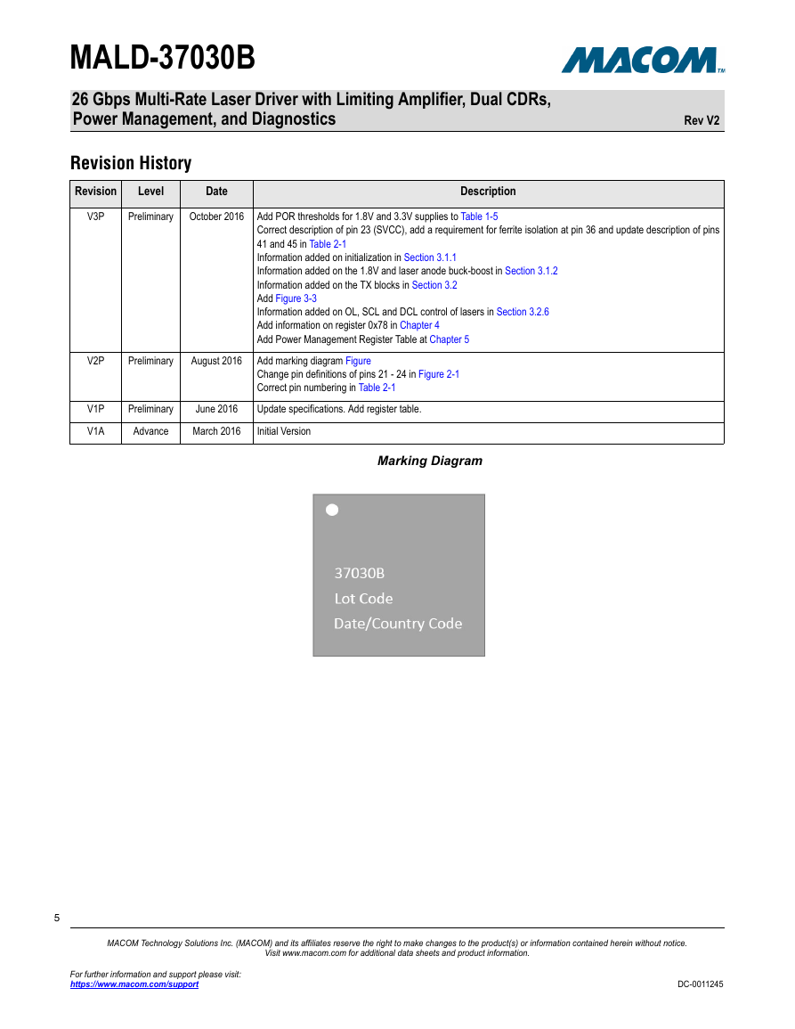
Marking Diagram
5
MACOM Technology Solutions Inc. (MACOM) and its affiliates reserve the right to make changes to the product(s) or information contained herein without notice.
Visit www.macom.com for additional data sheets and product information.
For further information and support please visit:
https://www.macom.com/support
DC-0011245
�
MALD-37030B
26 Gbps Multi-Rate Laser Driver with Limiting Amplifier, Dual CDRs,
Power Management, and Diagnostics
Rev V2
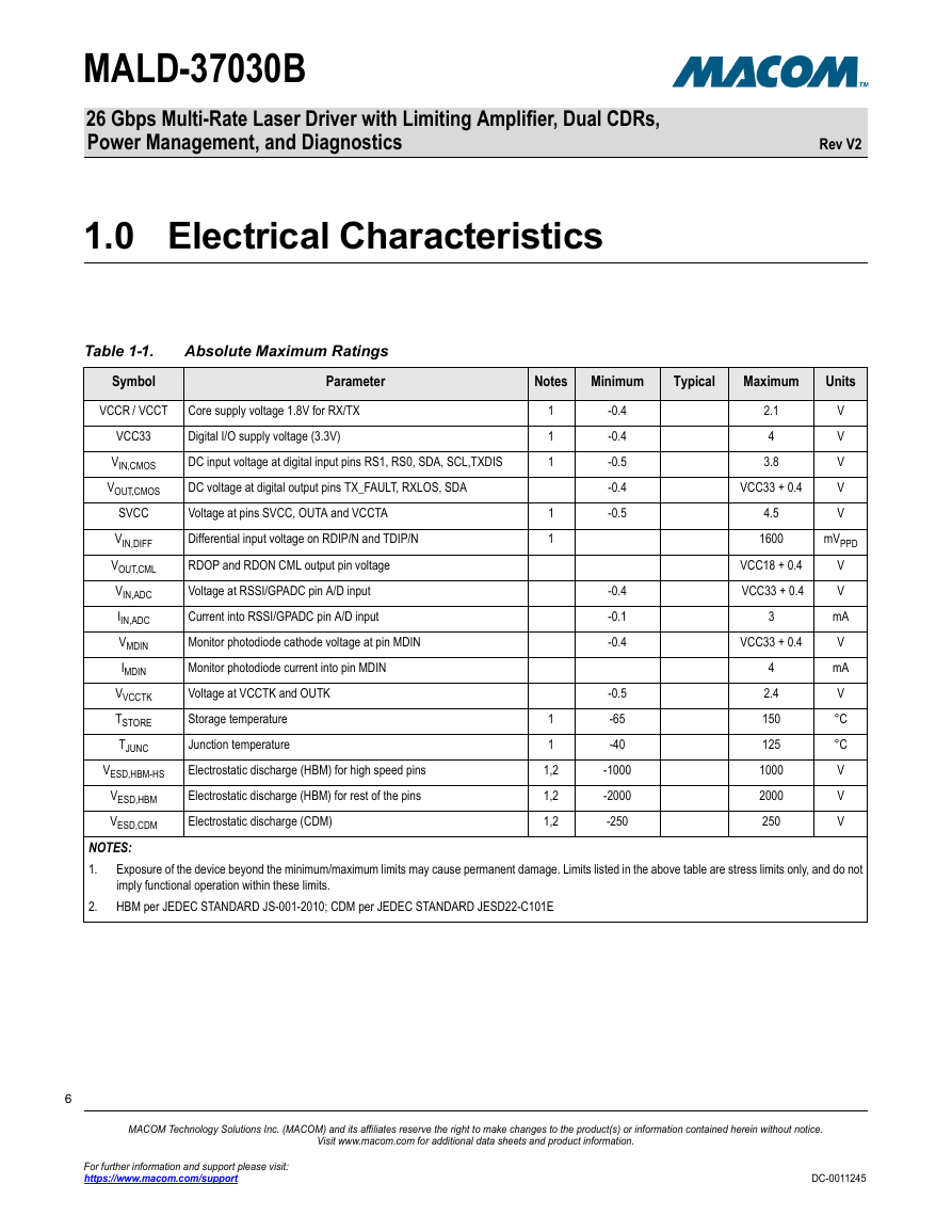
1.0 Electrical Characteristics
Table 1-1.
Symbol
Absolute Maximum Ratings
Parameter
Notes
Minimum
Typical
Maximum
Units
VCCR / VCCT
VCC33
VIN,CMOS
VOUT,CMOS
SVCC
VIN,DIFF
VOUT,CML
VIN,ADC
IIN,ADC
VMDIN
IMDIN
VVCCTK
TSTORE
TJUNC
VESD,HBM-HS
VESD,HBM
VESD,CDM
Core supply voltage 1.8V for RX/TX
Digital I/O supply voltage (3.3V)
DC input voltage at digital input pins RS1, RS0, SDA, SCL,TXDIS
DC voltage at digital output pins TX_FAULT, RXLOS, SDA
Voltage at pins SVCC, OUTA and VCCTA
Differential input voltage on RDIP/N and TDIP/N
RDOP and RDON CML output pin voltage
Voltage at RSSI/GPADC pin A/D input
Current into RSSI/GPADC pin A/D input
Monitor photodiode cathode voltage at pin MDIN
Monitor photodiode current into pin MDIN
Voltage at VCCTK and OUTK
Storage temperature
Junction temperature
Electrostatic discharge (HBM) for high speed pins
Electrostatic discharge (HBM) for rest of the pins
Electrostatic discharge (CDM)
1
1
1
1
1
1
1
1,2
1,2
1,2
-0.4
-0.4
-0.5
-0.4
-0.5
-0.4
-0.1
-0.4
-0.5
-65
-40
-1000
-2000
-250
2.1
4
3.8
VCC33 + 0.4
4.5
1600
VCC18 + 0.4
VCC33 + 0.4
3
VCC33 + 0.4
4
2.4
150
125
1000
2000
250
V
V
V
V
V
mVPPD
V
V
mA
V
mA
V
°C
°C
V
V
V
Exposure of the device beyond the minimum/maximum limits may cause permanent damage. Limits listed in the above table are stress limits only, and do not
imply functional operation within these limits.
HBM per JEDEC STANDARD JS-001-2010; CDM per JEDEC STANDARD JESD22-C101E
NOTES:
1.
2.
6
MACOM Technology Solutions Inc. (MACOM) and its affiliates reserve the right to make changes to the product(s) or information contained herein without notice.
Visit www.macom.com for additional data sheets and product information.
For further information and support please visit:
https://www.macom.com/support
DC-0011245
�
MALD-37030B
26 Gbps Multi-Rate Laser Driver with Limiting Amplifier, Dual CDRs,
Power Management, and Diagnostics
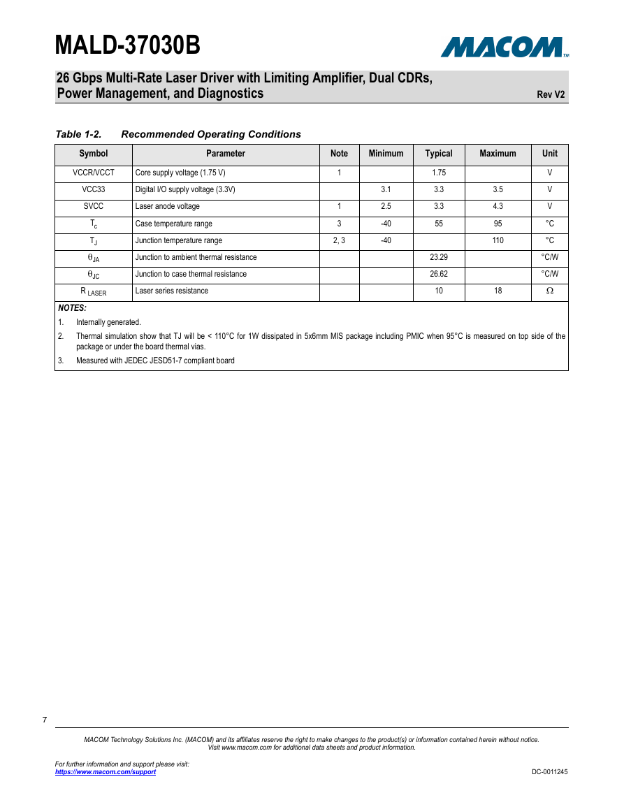
Table 1-2.
Symbol
VCCR/VCCT
VCC33
SVCC
Tc
TJ
JA
JC
R LASER
Recommended Operating Conditions
Parameter
Note
Minimum
Typical
Maximum
Core supply voltage (1.75 V)
Digital I/O supply voltage (3.3V)
Laser anode voltage
Case temperature range
Junction temperature range
Junction to ambient thermal resistance
Junction to case thermal resistance
Laser series resistance
1
1
3
2, 3
3.1
2.5
-40
-40
1.75
3.3
3.3
55
23.29
26.62
10
3.5
4.3
95
110
18
Rev V2
Unit
V
V
V
°C
°C
°C/W
°C/W
NOTES:
1.
2.
Internally generated.
Thermal simulation show that TJ will be < 110°C for 1W dissipated in 5x6mm MIS package including PMIC when 95°C is measured on top side of the
package or under the board thermal vias.
Measured with JEDEC JESD51-7 compliant board
3.
7
MACOM Technology Solutions Inc. (MACOM) and its affiliates reserve the right to make changes to the product(s) or information contained herein without notice.
Visit www.macom.com for additional data sheets and product information.
For further information and support please visit:
https://www.macom.com/support
DC-0011245
�
MALD-37030B
26 Gbps Multi-Rate Laser Driver with Limiting Amplifier, Dual CDRs,
Power Management, and Diagnostics
Rev V2
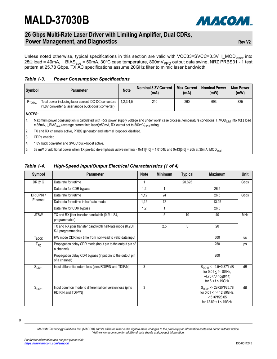
Unless noted otherwise, typical specifications in this section are valid with VCC33=SVCC=3.3V, I_MODlaser into
25 load = 40mA, I_BIASave = 50mA, 30°C case temperature, 800mVPPD output data swing, NRZ PRBS31 - 1 test
pattern at 25.78 Gbps. TX AC specifications assume 20GHz filter to mimic laser bandwidth.
Table 1-3.
Power Consumption Specifications
Symbol
Parameter
Note
Nominal 3.3V Current
(mA)
Max Current
(mA)
Nominal Power
(mW)
Max Power
(mW)
PTOTAL
Total power including laser current, DC-DC converters
(1.8V converter & laser anode buck-boost converter)
1,2,3,4,5
210
260
693
825
NOTES:
1.
Maximum power consumption is calculated with +5% power supply voltage and under worst case process, temperature conditions. I_MODtotal into 10 load
= 35mA, I_BIASave (average current into laser)=50mA, RX output set to 800mVPPD swing.
TX and RX channels active, PRBS generator and internal loopback disabled.
CDRs enabled.
1.8V buck converter and SVCC buck-boost active.
33 mW of additional power when TX pre-tap de-emphasis active nominal - 0x41[4:0] = 1 0101b and 0x43[5:0] = 20h at 35mA IMODtotal.
2.
3.
4.
5.
High-Speed Input/Output Electrical Characteristics (1 of 4)
Parameter
Data rate for retime
Data rate for CDR bypass
Data rate for retime
Data rate for retime in half-rate mode
Data rate for CDR bypass
TX and RX jitter transfer bandwidth (0.2UI SJ,
programmable)
TX and RX jitter transfer bandwidth half-rate mode (0.2UI
SJ, programmable)
HW mode CDR lock time from non-valid to valid data input
Propagation delay CDR mode (input pin to the output pin of
a channel)
Propagation delay CDR bypass (input pin to the output pin
of a channel)
Input differential return loss (pins RDIP/N and TDIP/N)
Input common mode to differential conversion loss (pins
RDIP/N and TDIP/N)
Note
1
1,2
1,12
1,12
1,2
3
3
Minimum
Typical
20.625
Maximum
1
24
12
1
5
2.5
10
5
26.5
26.5
13.25
26.5
40
20
500
250
200
SDD11 < --9.5+0.37*f dB
for 0.01 < f < 8GHz,
-4.75+7.4*log(f/14)
for 8 < f < 19GHz
SDC11 <- 22+20*f/25.78
for 0.01 < f < 12.89GHz,
-15+6*f/28.05
for 12.89 < f < 19GHz
Unit
Gbps
Gbps
MHz
us
ps
dB
dB
Table 1-4.
Symbol
DR 21G
DR CPRI /
Ethernet
JTBW
TLOCK
TPD
SDD11
SDC11
8
MACOM Technology Solutions Inc. (MACOM) and its affiliates reserve the right to make changes to the product(s) or information contained herein without notice.
Visit www.macom.com for additional data sheets and product information.
For further information and support please visit:
https://www.macom.com/support
DC-0011245
�



 2023年江西萍乡中考道德与法治真题及答案.doc
 2012年重庆南川中考生物真题及答案.doc
 2013年江西师范大学地理学综合及文艺理论基础考研真题.doc
 2020年四川甘孜小升初语文真题及答案I卷.doc
 2020年注册岩土工程师专业基础考试真题及答案.doc
 2023-2024学年福建省厦门市九年级上学期数学月考试题及答案.doc
 2021-2022学年辽宁省沈阳市大东区九年级上学期语文期末试题及答案.doc
 2022-2023学年北京东城区初三第一学期物理期末试卷及答案.doc
 2018上半年江西教师资格初中地理学科知识与教学能力真题及答案.doc
 2012年河北国家公务员申论考试真题及答案-省级.doc
 2020-2021学年江苏省扬州市江都区邵樊片九年级上学期数学第一次质量检测试题及答案.doc
 2022下半年黑龙江教师资格证中学综合素质真题及答案.doc