Revision History
About this Document
Introduction
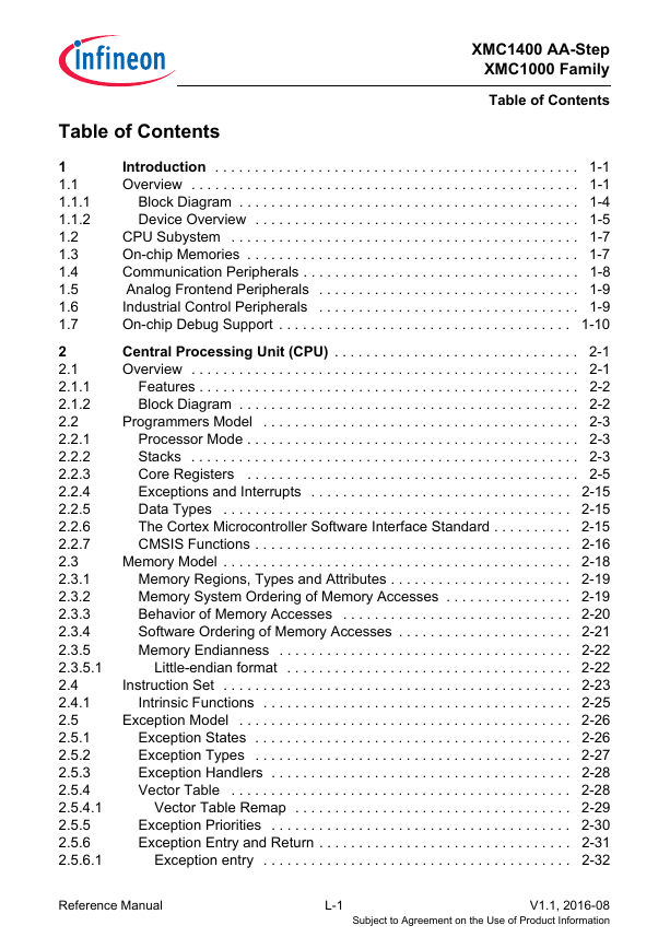
1 Introduction
1.1 Overview
1.1.1 Block Diagram
1.1.2 Device Overview
1.2 CPU Subystem
1.3 On-chip Memories
1.4 Communication Peripherals
1.5 Analog Frontend Peripherals
1.6 Industrial Control Peripherals
1.7 On-chip Debug Support
CPU Subsystem
2 Central Processing Unit (CPU)
2.1 Overview
2.1.1 Features
2.1.2 Block Diagram
2.2 Programmers Model
2.2.1 Processor Mode
2.2.2 Stacks
2.2.3 Core Registers
2.2.4 Exceptions and Interrupts
2.2.5 Data Types
2.2.6 The Cortex Microcontroller Software Interface Standard
2.2.7 CMSIS Functions
2.3 Memory Model
2.3.1 Memory Regions, Types and Attributes
2.3.2 Memory System Ordering of Memory Accesses
2.3.3 Behavior of Memory Accesses
2.3.4 Software Ordering of Memory Accesses
2.3.5 Memory Endianness
2.3.5.1 Little-endian format
2.4 Instruction Set
2.4.1 Intrinsic Functions
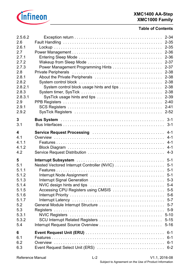
2.5 Exception Model
2.5.1 Exception States
2.5.2 Exception Types
2.5.3 Exception Handlers
2.5.4 Vector Table
2.5.4.1 Vector Table Remap
2.5.5 Exception Priorities
2.5.6 Exception Entry and Return
2.5.6.1 Exception entry
2.5.6.2 Exception return
2.6 Fault Handling
2.6.1 Lockup
2.7 Power Management
2.7.1 Entering Sleep Mode
2.7.2 Wakeup from Sleep Mode
2.7.3 Power Management Programming Hints
2.8 Private Peripherals
2.8.1 About the Private Peripherals
2.8.2 System control block
2.8.2.1 System control block usage hints and tips
2.8.3 System timer, SysTick
2.8.3.1 SysTick usage hints and tips
2.9 PPB Registers
2.9.1 SCS Registers
2.9.2 SysTick Registers
3 Bus System
3.1 Bus Interfaces
4 Service Request Processing
4.1 Overview
4.1.1 Features
4.1.2 Block Diagram
4.2 Service Request Distribution
5 Interrupt Subsystem
5.1 Nested Vectored Interrupt Controller (NVIC)
5.1.1 Features
5.1.2 Interrupt Node Assignment
5.1.3 Interrupt Signal Generation
5.1.4 NVIC design hints and tips
5.1.5 Accessing CPU Registers using CMSIS
5.1.6 Interrupt Priority
5.1.7 Interrupt Latency
5.2 General Module Interrupt Structure
5.3 Registers
5.3.1 NVIC Registers
5.3.2 SCU Interrupt Related Registers
5.4 Interrupt Request Source Overview
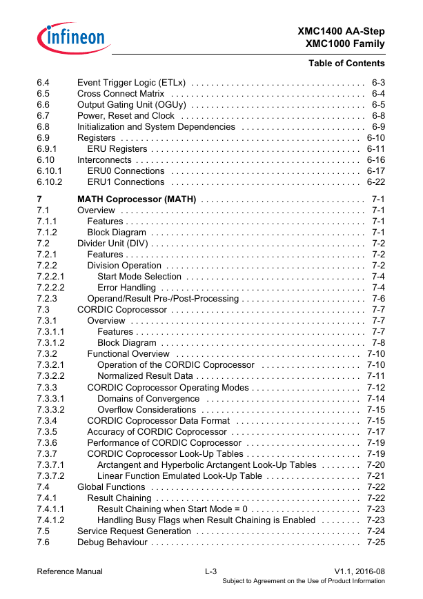
6 Event Request Unit (ERU)
6.1 Features
6.2 Overview
6.3 Event Request Select Unit (ERS)
6.4 Event Trigger Logic (ETLx)
6.5 Cross Connect Matrix
6.6 Output Gating Unit (OGUy)
6.7 Power, Reset and Clock
6.8 Initialization and System Dependencies
6.9 Registers
6.9.1 ERU Registers
6.10 Interconnects
6.10.1 ERU0 Connections
6.10.2 ERU1 Connections
7 MATH Coprocessor (MATH)
7.1 Overview
7.1.1 Features
7.1.2 Block Diagram
7.2 Divider Unit (DIV)
7.2.1 Features
7.2.2 Division Operation
7.2.2.1 Start Mode Selection
7.2.2.2 Error Handling
7.2.3 Operand/Result Pre-/Post-Processing
7.3 CORDIC Coprocessor
7.3.1 Overview
7.3.1.1 Features
7.3.1.2 Block Diagram
7.3.2 Functional Overview
7.3.2.1 Operation of the CORDIC Coprocessor
7.3.2.2 Normalized Result Data
7.3.3 CORDIC Coprocessor Operating Modes
7.3.3.1 Domains of Convergence
7.3.3.2 Overflow Considerations
7.3.4 CORDIC Coprocessor Data Format
7.3.5 Accuracy of CORDIC Coprocessor
7.3.6 Performance of CORDIC Coprocessor
7.3.7 CORDIC Coprocessor Look-Up Tables
7.3.7.1 Arctangent and Hyperbolic Arctangent Look-Up Tables
7.3.7.2 Linear Function Emulated Look-Up Table
7.4 Global Functions
7.4.1 Result Chaining
7.4.1.1 Result Chaining when Start Mode = 0
7.4.1.2 Handling Busy Flags when Result Chaining is Enabled
7.5 Service Request Generation
7.6 Debug Behaviour
7.7 Power, Reset and Clock
7.8 Registers
7.8.1 Global Registers Description
7.8.2 Divider Registers Description
7.8.3 CORDIC Registers Description
7.9 Interconnects
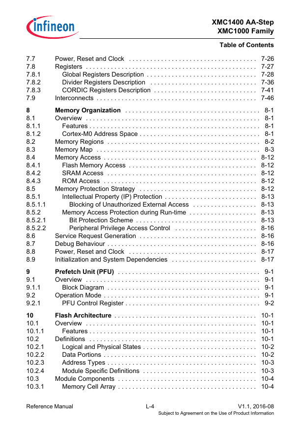
On-Chip Memories
8 Memory Organization
8.1 Overview
8.1.1 Features
8.1.2 Cortex-M0 Address Space
8.2 Memory Regions
8.3 Memory Map
8.4 Memory Access
8.4.1 Flash Memory Access
8.4.2 SRAM Access
8.4.3 ROM Access
8.5 Memory Protection Strategy
8.5.1 Intellectual Property (IP) Protection
8.5.1.1 Blocking of Unauthorized External Access
8.5.2 Memory Access Protection during Run-time
8.5.2.1 Bit Protection Scheme
8.5.2.2 Peripheral Privilege Access Control
8.6 Service Request Generation
8.7 Debug Behaviour
8.8 Power, Reset and Clock
8.9 Initialization and System Dependencies
9 Prefetch Unit (PFU)
9.1 Overview
9.1.1 Block Diagram
9.2 Operation Mode
9.2.1 PFU Control Register
10 Flash Architecture
10.1 Overview
10.1.1 Features
10.2 Definitions
10.2.1 Logical and Physical States
10.2.2 Data Portions
10.2.3 Address Types
10.2.4 Module Specific Definitions
10.3 Module Components
10.3.1 Memory Cell Array
10.3.1.1 Page
10.3.1.2 Sector
10.4 Functional Description
10.4.1 SFR Accesses
10.4.2 Memory Read
10.4.3 Memory Write
10.4.4 Memory Erase
10.4.5 Sector Erase
10.4.6 Verify
10.4.7 Erase-Protection and Write-Protection
10.5 Properties and Implementation of Error Correcting Code (ECC)
10.6 Service Request Generation
10.7 Power, Reset and Clock
10.7.1 Power Supply
10.7.2 Power Saving Modes
10.7.2.1 NVM Idle Mode
10.7.2.2 NVM Sleep Mode
10.7.3 Reset
10.7.4 Clock
10.8 Registers
10.8.1 NVM Registers
10.9 Example Sequences
10.9.1 Writing to Memory
10.9.1.1 Writing a Single Block
10.9.1.2 Writing Blocks
10.9.2 Erasing Memory
10.9.2.1 Erasing a Single Page
10.9.2.2 Erasing Pages
10.9.2.3 Erasing a Single Sector
10.9.2.4 Erasing Sectors
10.9.3 Verifying Memory
10.9.3.1 Verifying a Single Block
10.9.3.2 Verifying Blocks
10.9.4 Writing to an Already Written Block
10.9.5 Sleep Mode
10.9.6 Timing
11 Peripheral Access Unit (PAU)
11.1 Overview
11.1.1 Features
11.2 Peripheral Privilege Access Control
11.3 Peripheral Availability and Memory Size
11.4 Service Request Generation
11.5 Debug Behaviour
11.6 Power, Reset and Clock
11.7 Initialization and System Dependencies
11.8 PAU Registers
11.8.1 Peripheral Privilege Access Registers (PRIVDISn)
11.8.2 Peripheral Availability Registers (AVAILn)
11.8.3 Memory Size Registers
System Control
12 Window Watchdog Timer (WDT)
12.1 Overview
12.1.1 Features
12.1.2 Block Diagram
12.2 Time-Out Mode
12.3 Pre-warning Mode
12.4 Bad Service Operation
12.5 Service Request Processing
12.6 Debug Behavior
12.7 Power, Reset and Clock
12.8 Initialization and Control Sequence
12.8.1 Initialization & Start of Operation
12.8.2 Software Stop & Resume Operation
12.8.3 Enter Sleep/Deep-Sleep & Resume Operation
12.8.4 Pre-warning Alarm Handling
12.9 WDT Registers
12.9.1 Registers Description
12.10 Interconnects
13 Real Time Clock (RTC)
13.1 Overview
13.1.1 Features
13.1.2 Block Diagram
13.2 RTC Operation
13.3 Register Access Operations
13.4 Service Request Processing
13.4.1 Periodic Service Request
13.4.2 Timer Alarm Service Request
13.5 Debug Behavior
13.6 Power, Reset and Clock
13.7 Initialization and Control Sequence
13.7.1 Initialization & Start of Operation
13.7.2 Configure and Enable Periodic Event
13.7.3 Configure and Enable Timer Event
13.8 RTC Registers
13.8.1 Registers Description
13.9 Interconnects
14 System Control Unit (SCU)
14.1 Overview
14.1.1 Features
14.1.2 Block Diagram
14.2 Miscellaneous Control Functions (GCU)
14.2.1 Service Requests Handling
14.2.1.1 Service Request Sources
14.2.2 SRAM Memory Content Protection
14.2.3 Summary of ID
14.2.4 Boot via Pins
14.3 Power Management (PCU)
14.3.1 Functional Description
14.3.2 System States
14.3.3 Embedded Voltage Regulator (EVR)
14.3.4 Power-on Reset
14.3.5 Power Validation
14.3.6 Supply Voltage Monitoring
14.3.7 VDDC Response During Load Change
14.3.8 Flash Power Control
14.4 Reset Control (RCU)
14.4.1 Functional Description
14.4.2 Reset Status
14.5 Clock Control (CCU)
14.5.1 Features
14.5.2 Clock System and Control
14.5.2.1 DCO1 Oscillator Watchdog
14.5.2.2 Loss of DCO1 Clock Detection and Recovery
14.5.2.3 Standby Clock Failure
14.5.2.4 XTAL Oscillator Watchdog
14.5.2.5 Loss of external OSC_HP Clock Detection and Recovery
14.5.2.6 Startup Control for System Clock
14.5.2.7 DCLK input - External Clock via OSC_HP
14.5.3 Clock Gating Control
14.5.4 Calibrating DCO1 based on Temperature
14.5.5 Automatic DCO1 Calibration based on External Reference
14.6 Service Request Generation
14.7 Debug Behavior
14.8 Power, Reset and Clock
14.9 Registers
14.9.1 PCU Registers (ANACTRL)
14.9.2 PCU Registers (SCU)
14.9.3 CCU Registers (SCU)
14.9.4 CCU Registers (ANACTRL)
14.9.5 RCU Registers (SCU)
14.9.6 GCU Registers (SCU)
15 Pseudo Random Number Generator (PRNG)
15.1 Overview
15.1.1 Features
15.2 Description of Operation Modes
15.2.1 Key Loading Mode
15.2.2 Streaming Mode
15.2.3 Refreshing and Restarting a Random Bit Stream
15.3 Service Request Generation
15.4 Debug Behavior
15.5 Power, Reset and Clock
15.6 Initialization and System Dependencies
15.7 Registers
15.7.1 Data Registers
15.7.2 Control Registers
Communication Peripherals
16 LED and Touch-Sense (LEDTS)
16.1 Overview
16.1.1 Features
16.1.2 Block Diagram
16.2 Functional Overview
16.3 LED Drive Mode
16.3.1 LED Pin Assignment and Current Capability
16.4 Touch-Sense Mode
16.4.1 Finger Sensing
16.5 Operating both LED Drive and Touch-Sense Modes
16.6 Service Request Processing
16.7 Debug Behavior
16.8 Power, Reset and Clock
16.9 Initialisation and System Dependencies
16.9.1 Function Enabling
16.9.2 Interpretation of Bit Field FNCOL
16.9.3 LEDTS Timing Calculations
16.9.4 Time-Multiplexed LED and Touch-Sense Functions on Pin
16.9.5 LEDTS Pin Control
16.9.6 Software Hints
16.9.7 Hardware Design Hints
16.10 Multiple Kernels Usage and Synchronization
16.11 Registers
16.11.1 Registers Description
16.12 Interconnects
17 Universal Serial Interface Channel (USIC)
17.1 Overview
17.1.1 Features
17.2 Operating the USIC
17.2.1 USIC Structure Overview
17.2.1.1 Channel Structure
17.2.1.2 Input Stages
17.2.1.3 Output Signals
17.2.1.4 Baud Rate Generator
17.2.1.5 Channel Events and Interrupts
17.2.1.6 Data Shifting and Handling
17.2.2 Operating the USIC Communication Channel
17.2.2.1 Protocol Control and Status
17.2.2.2 Mode Control
17.2.3 Operating the Input Stages
17.2.3.1 General Input Structure
17.2.3.2 Input Selection
17.2.3.3 Input Conditioning
17.2.3.4 Digital Filter
17.2.3.5 Edge Detection
17.2.3.6 Selected Input Monitoring
17.2.3.7 Loop Back Mode
17.2.3.8 Delay Compensation in DX1
17.2.4 Operating the Baud Rate Generator
17.2.4.1 Fractional Divider
17.2.4.2 External Frequency Input
17.2.4.3 Divider Mode Counter
17.2.4.4 Capture Mode Timer
17.2.4.5 Time Quanta Counter
17.2.4.6 Master and Shift Clock Output Configuration
17.2.5 Operating the Transmit Data Path
17.2.5.1 Transmit Buffering
17.2.5.2 Transmit Data Shift Mode
17.2.5.3 Transmit Control Information
17.2.5.4 Transmit Data Validation
17.2.6 Operating the Receive Data Path
17.2.6.1 Receive Buffering
17.2.6.2 Receive Data Shift Mode
17.2.6.3 Baud Rate Constraints
17.2.7 Hardware Port Control
17.2.8 Operating the FIFO Data Buffer
17.2.8.1 FIFO Buffer Partitioning
17.2.8.2 Transmit FIFO Buffer Modes
17.2.8.3 Transmit Buffer Events and Interrupts
17.2.8.4 Transmit FIFO Buffer Usage Example
17.2.8.5 Receive FIFO Buffer Modes
17.2.8.6 Receive Buffer Events and Interrupts
17.2.8.7 Receive FIFO Buffer in Filling Level Mode Usage Example
17.2.8.8 FIFO Buffer Bypass
17.2.8.9 FIFO Access Constraints
17.2.8.10 Handling of FIFO Transmit Control Information
17.3 Asynchronous Serial Channel (ASC = UART)
17.3.1 Signal Description
17.3.1.1 ASC Full-Duplex Communication
17.3.1.2 ASC Half-Duplex Communication
17.3.2 Frame Format
17.3.2.1 Idle Detection
17.3.2.2 Start Bit Detection
17.3.2.3 Data Field
17.3.2.4 Parity Bit
17.3.2.5 Stop Bit(s)
17.3.3 Operating the ASC
17.3.3.1 Bit Timing
17.3.3.2 Baud Rate Generation
17.3.3.3 Automatic Shadow Mechanism
17.3.3.4 Mode Control Behavior
17.3.3.5 Disabling ASC Mode
17.3.3.6 Data Transfer Interrupt Handling
17.3.3.7 Protocol Interrupt Events
17.3.3.8 Baud Rate Generator Interrupt Handling
17.3.3.9 Protocol-Related Argument and Error
17.3.3.10 Receive FIFO Buffer Handling
17.3.3.11 Data Flow Handling
17.3.3.12 Initialization Code Example
17.3.4 Additional Features
17.3.4.1 Noise Detection
17.3.4.2 Collision Detection
17.3.4.3 Pulse Shaping
17.3.4.4 End of Frame Control
17.3.4.5 Sync-Break Detection
17.3.4.6 Transfer Status Indication
17.3.5 Hardware LIN Support
17.4 Synchronous Serial Channel (SSC)
17.4.1 Signal Description
17.4.1.1 Transmit and Receive Data Signals
17.4.1.2 Shift Clock Signals
17.4.1.3 Slave Select Signals
17.4.2 Operating the SSC
17.4.2.1 Automatic Shadow Mechanism
17.4.2.2 Mode Control Behavior
17.4.2.3 Disabling SSC Mode
17.4.2.4 Data Frame Control
17.4.2.5 Parity Mode
17.4.2.6 Data Transfer Interrupt Handling
17.4.2.7 Protocol-Related Argument and Error
17.4.2.8 Receive Buffer Handling
17.4.3 Operating the SSC in Master Mode
17.4.3.1 Baud Rate Generation
17.4.3.2 MSLS Generation and Slave Select Delays
17.4.3.3 Configuration of Slave Select Delays
17.4.3.4 Automatic Slave Select Update
17.4.3.5 Protocol Interrupt Events
17.4.3.6 End-of-Frame Control
17.4.3.7 Data Flow Handling
17.4.3.8 Initialization Code Example
17.4.4 Operating the SSC in Slave Mode
17.4.4.1 Protocol Interrupts
17.4.4.2 End-of-Frame Control
17.4.4.3 Data Flow Handling
17.4.4.4 Initialization Code Example
17.4.5 Multi-IO SSC Protocols
17.4.5.1 Operating the SSC in Multi-IO Modes
17.4.5.2 Quad-SSC Example
17.4.6 SSC Timing Considerations
17.4.6.1 Closed-loop Delay
17.4.6.2 Delay Compensation in Master Mode
17.4.6.3 Complete Closed-loop Delay Compensation
17.5 Inter-IC Bus Protocol (IIC)
17.5.1 Introduction
17.5.1.1 Signal Description
17.5.1.2 Symbols
17.5.1.3 Frame Format
17.5.2 Symbol Timing
17.5.2.1 Start Symbol
17.5.2.2 Repeated Start Symbol
17.5.2.3 Stop Symbol
17.5.2.4 Data Bit Symbol
17.5.3 Operating the IIC
17.5.3.1 Baud Rate Generation
17.5.3.2 Transmission Chain
17.5.3.3 Byte Stretching
17.5.3.4 Master Arbitration
17.5.3.5 Not Acknowledge and Error Conditions
17.5.3.6 Mode Control Behavior
17.5.3.7 Data Transfer Interrupt Handling
17.5.3.8 IIC Protocol Interrupt Events
17.5.3.9 Receiver Address Acknowledge
17.5.3.10 Receiver Handling
17.5.3.11 Receiver Status Information
17.5.3.12 IIC Initialization Code Example
17.5.4 Data Flow Handling
17.5.4.1 Transmit Data Formats
17.5.4.2 Valid Master Transmit Data Formats
17.5.4.3 Master Transmit/Receive Modes
17.5.4.4 Slave Transmit/Receive Modes
17.6 Inter-IC Sound Bus Protocol (IIS)
17.6.1 Introduction
17.6.1.1 Signal Description
17.6.1.2 Protocol Overview
17.6.1.3 Transfer Delay
17.6.1.4 Connection of External Audio Components
17.6.2 Operating the IIS
17.6.2.1 Frame Length and Word Length Configuration
17.6.2.2 Automatic Shadow Mechanism
17.6.2.3 Mode Control Behavior
17.6.2.4 Transfer Delay
17.6.2.5 Data Transfer Interrupt Handling
17.6.2.6 Protocol-Related Argument and Error
17.6.2.7 Transmit Data Handling
17.6.2.8 Receive Buffer Handling
17.6.2.9 Loop-Delay Compensation
17.6.3 Operating the IIS in Master Mode
17.6.3.1 Baud Rate Generation
17.6.3.2 WA Generation
17.6.3.3 Master Clock Output
17.6.3.4 Protocol Interrupt Events
17.6.3.5 Initialization Code Example
17.6.4 Operating the IIS in Slave Mode
17.6.4.1 Protocol Interrupt Events
17.6.4.2 Initialization Code Example
17.7 Service Request Generation
17.7.1 General Channel Events and Interrupts
17.7.2 Data Transfer Events and Interrupts
17.7.3 Baud Rate Generator Event and Interrupt
17.7.4 Protocol-specific Events and Interrupts
17.8 Debug Behaviour
17.9 Power, Reset and Clock
17.10 Initialization and System Dependencies
17.11 Registers
17.11.1 Address Map
17.11.2 Module Identification Registers
17.11.3 Channel Control and Configuration Registers
17.11.3.1 Channel Control Register
17.11.3.2 Channel Configuration Register
17.11.3.3 Kernel State Configuration Register
17.11.3.4 Interrupt Node Pointer Register
17.11.4 Protocol Related Registers
17.11.4.1 Protocol Control Registers
17.11.4.2 ASC Protocol Control Register
17.11.4.3 SSC Protocol Control Registers
17.11.4.4 IIC Protocol Control Registers
17.11.4.5 IIS Protocol Control Registers
17.11.4.6 Protocol Status Register
17.11.4.7 ASC Protocol Status Register
17.11.4.8 SSC Protocol Status Register
17.11.4.9 IIC Protocol Status Register
17.11.4.10 IIS Protocol Status Register
17.11.4.11 Protocol Status Clear Register
17.11.5 Input Stage Register
17.11.5.1 Input Control Registers
17.11.6 Baud Rate Generator Registers
17.11.6.1 Fractional Divider Register
17.11.6.2 Baud Rate Generator Register
17.11.6.3 Capture Mode Timer Register
17.11.7 Transfer Control and Status Registers
17.11.7.1 Shift Control Register
17.11.7.2 Transmission Control and Status Register
17.11.7.3 Flag Modification Registers
17.11.8 Data Buffer Registers
17.11.8.1 Transmit Buffer Locations
17.11.8.2 Receive Buffer Registers RBUF0, RBUF1
17.11.8.3 Receive Buffer Registers RBUF, RBUFD, RBUFSR
17.11.9 FIFO Buffer and Bypass Registers
17.11.9.1 Bypass Registers
17.11.9.2 General FIFO Buffer Control Registers
17.11.9.3 Transmit FIFO Buffer Control Registers
17.11.9.4 Receive FIFO Buffer Control Registers
17.11.9.5 FIFO Buffer Data Registers
17.11.9.6 FIFO Buffer Pointer Registers
17.12 Interconnects
17.12.1 USIC0 Module Interconnects
17.12.1.1 USIC0 Channel 0 Interconnects
17.12.1.2 USIC0 Channel 1 Interconnects
17.12.1.3 USIC0 Global Interconnects
17.12.2 USIC1 Module Interconnects
17.12.2.1 USIC1 Channel 0 Interconnects
17.12.2.2 USIC1 Channel 1 Interconnects
17.12.2.3 USIC1 Global Interconnects
18 Controller Area Network Controller (MultiCAN+)
18.1 CAN Basics
18.1.1 Addressing and Bus Arbitration
18.1.2 CAN Frame Types
18.1.2.1 Data Frames
18.1.2.2 Remote Frames
18.1.2.3 Error Frames
18.1.3 The Nominal Bit Time
18.1.4 Error Detection and Error Handling
18.2 Overview
18.2.1 Features List
18.3 MultiCAN+ Kernel Functional Description
18.3.1 Module Structure
18.3.2 Clock Control
18.3.3 Port Input Control
18.3.4 CAN Node Control
18.3.4.1 Bit Timing Unit
18.3.4.2 Bitstream Processor
18.3.4.3 Error Handling Unit
18.3.4.4 CAN Frame Counter
18.3.4.5 CAN Node Interrupts
18.3.5 Message Object List Structure
18.3.5.1 Basics
18.3.5.2 List of Unallocated Elements
18.3.5.3 Connection to the CAN Nodes
18.3.5.4 List Command Panel
18.3.6 CAN Node Analyzer Mode
18.3.6.1 Analyzer Mode
18.3.6.2 Loop-Back Mode
18.3.6.3 Bit Timing Analysis
18.3.7 Message Acceptance Filtering
18.3.7.1 Receive Acceptance Filtering
18.3.7.2 Transmit Acceptance Filtering
18.3.8 Message Postprocessing
18.3.8.1 Message Object Interrupts
18.3.8.2 Pending Messages
18.3.9 Message Object Data Handling
18.3.9.1 Frame Reception
18.3.9.2 Frame Transmission
18.3.10 Message Object Functionality
18.3.10.1 Standard Message Object
18.3.10.2 Single Data Transfer Mode
18.3.10.3 Single Transmit Trial
18.3.10.4 Message Object FIFO Structure
18.3.10.5 Receive FIFO
18.3.10.6 Transmit FIFO
18.3.10.7 Gateway Mode
18.3.10.8 Foreign Remote Requests
18.4 Use Case Example MultiCAN+
18.5 MultiCAN+ Kernel Registers
18.5.1 Global Module Registers
18.5.2 CAN Node Registers
18.5.3 Message Object Registers
18.6 MultiCAN+ Module Implementation
18.6.1 Interfaces of the MultiCAN+ Module
18.6.2 MultiCAN+ Module External Registers
18.6.3 Module Clock Generation
18.6.3.1 Clock Selection
18.6.3.2 Fractional Divider
18.6.4 Port and I/O Line Control
18.6.4.1 Input/Output Function Selection in Ports
18.6.4.2 Node Receive Input Selection
18.6.4.3 Connections to Interrupt Router Inputs
18.6.4.4 Connections to ERU
18.6.5 Interrupt Control
18.6.6 MultiCAN+ Module Register Address Map
Analog Peripherals
19 Versatile Analog-to-Digital Converter (VADC)
19.1 Overview
19.2 Introduction and Basic Structure
19.3 Electrical Models
19.4 Configuration of General Functions
19.4.1 General Clocking Scheme and Control
19.4.2 Register Access Control
19.4.3 Priority Channel and Result Register Assignment
19.5 Analog Module Activation and Control
19.5.1 Analog Converter Control
19.5.2 Converter Handling in Deep Sleep Mode
19.5.3 Calibration
19.5.4 Reference Voltage Selection
19.5.5 Sigma-Delta-Loop Function
19.6 Conversion Request Generation
19.6.1 Queued Request Source Handling
19.6.2 Channel Scan Request Source Handling
19.7 Request Source Arbitration
19.7.1 Arbiter Operation and Configuration
19.7.2 Conversion Start Mode
19.8 Analog Input Channel Configuration
19.8.1 Channel Parameters
19.8.2 Alias Feature
19.8.3 Conversion Modes
19.8.4 Compare with Standard Conversions (Limit Checking)
19.8.5 Utilizing Fast Compare Mode
19.8.6 Boundary Flag Control
19.9 Conversion Scheduling
19.10 Conversion Timing
19.10.1 Timing Definition
19.10.2 Compatible Timing Mode
19.11 Conversion Result Handling
19.11.1 Storage of Conversion Results
19.11.2 Data Alignment
19.11.3 Wait-for-Read Mode
19.11.4 Result FIFO Buffer
19.11.5 Result Event Generation
19.11.6 Data Modification
19.12 Synchronization of Conversions
19.12.1 Synchronized Conversions for Parallel Sampling
19.12.2 Equidistant Sampling
19.13 Safety Features
19.13.1 Broken Wire Detection
19.13.2 Multiplexer Diagnostics
19.14 External Multiplexer Control
19.15 Service Request Generation
19.16 Registers
19.16.1 Module Identification
19.16.2 System Registers
19.16.3 General Registers
19.16.4 Arbitration and Source Registers
19.16.5 Channel Control Registers
19.16.6 Result Registers
19.16.7 Calibration Registers
19.16.8 Miscellaneous Registers
19.16.9 Service Request Registers
19.17 Interconnects
19.17.1 Product-Specific Configuration
19.17.2 Analog Module Connections in the XMC1400
19.17.3 Digital Module Connections in the XMC1400
20 Analog Comparator (ACMP) and Out of Range Comparator (ORC)
20.1 Overview
20.1.1 Features
20.2 Analog Comparator (ACMP)
20.3 Out of Range Comparator (ORC)
20.4 Service Request Generation
20.5 Debug Behavior
20.6 Registers
20.6.1 ORC Register
20.6.2 ACMP Registers
20.7 Interconnects
21 Temperature Sensor (DTS)
21.1 General Description
21.2 Service Request Generation
21.3 Registers
21.3.1 Registers
Industrial Control Peripherals
22 Capture/Compare Unit 4 (CCU4)
22.1 Overview
22.1.1 Features
22.1.2 Block Diagram
22.2 Functional Description
22.2.1 Timer Slice Overview
22.2.2 Timer Slice Input Selector
22.2.3 Timer Slice Connection Matrix
22.2.4 Timer Slice Core Functions
22.2.4.1 Starting/Stopping the Timer
22.2.4.2 Counting Modes Introduction
22.2.4.3 Edge Aligned Mode
22.2.4.4 Center Aligned Mode
22.2.4.5 Single Shot Mode
22.2.4.6 Calculating the PWM Period and Duty Cycle
22.2.4.7 Updating the Period, Duty Cycle and other PWM conditions
22.2.4.8 PWM Active/Passive Rules
22.2.4.9 Output PWM Path
22.2.5 Timer Slice External Functions
22.2.5.1 External Start/Stop
22.2.5.2 External Counting Direction
22.2.5.3 External Gating Signal
22.2.5.4 External Count Signal
22.2.5.5 External Load
22.2.5.6 External Capture
22.2.5.7 TRAP Function
22.2.5.8 Status Bit Override
22.2.5.9 External Modulation
22.2.6 Timer Slice Advanced Functions
22.2.6.1 Multi-Channel Control
22.2.6.2 Timer Concatenation
22.2.6.3 PWM Dithering
22.2.6.4 Capture Extended Read Back Mode
22.2.7 Clock Prescaler
22.2.7.1 Normal Prescaler Mode
22.2.7.2 Floating Prescaler Mode
22.2.8 CCU4 Usage
22.2.8.1 PWM Signal Generation
22.2.8.2 Prescaler Usage
22.2.8.3 PWM Dither
22.2.8.4 Capture Mode Usage
22.3 Service Request Generation
22.4 Debug Behavior
22.5 Power, Reset and Clock
22.5.1 Clocks
22.5.2 Power
22.6 Initialization and System Dependencies
22.6.1 Initialization Sequence
22.6.2 System Dependencies
22.7 Registers
22.7.1 Global Registers
22.7.2 Slice (CC4y) Registers
22.8 Interconnects
22.8.1 CCU40 Pins
22.8.2 CCU41 Pins
23 Capture/Compare Unit 8 (CCU8)
23.1 Overview
23.1.1 Features
23.1.2 Block Diagram
23.2 Functional Description
23.2.1 Timer Slice Overview
23.2.2 Timer Slice Input Selector
23.2.3 Timer Slice Connection Matrix
23.2.4 Timer Slice Core Functions
23.2.4.1 Starting/Stopping the Timer
23.2.4.2 Counting Modes Introduction
23.2.4.3 Edge Aligned Mode
23.2.4.4 Center Aligned Mode
23.2.4.5 Single Shot Mode
23.2.4.6 Dead Time Generation
23.2.4.7 Edge and Center Aligned Compare Modes
23.2.4.8 Calculating the PWM Period and Duty Cycle
23.2.4.9 Updating the Period, Duty Cycle and other PWM conditions
23.2.4.10 PWM Active/Passive Rules
23.2.4.11 Output PWM Path
23.2.5 Timer Slice External Functions
23.2.5.1 External Start/Stop
23.2.5.2 External Counting Direction
23.2.5.3 External Gating Signal
23.2.5.4 External Count Signal
23.2.5.5 External Load
23.2.5.6 External Capture
23.2.5.7 External Modulation
23.2.5.8 Trap Function
23.2.5.9 Status Bit Override
23.2.6 Timer Slice Advanced Functions
23.2.6.1 Multi-Channel Support
23.2.6.2 Timer Concatenation
23.2.6.3 PWM Dithering
23.2.6.4 Capture Extended Read Back Mode
23.2.6.5 Output Parity Checker
23.2.7 Clock Prescaler
23.2.7.1 Normal Prescaler Mode
23.2.7.2 Floating Prescaler Mode
23.2.8 CCU8 Usage
23.2.8.1 PWM Signal Generation
23.2.8.2 Prescaler Usage
23.2.8.3 PWM Dither
23.2.8.4 Capture Mode Usage
23.2.8.5 Parity Checker Usage
23.3 Service Request Generation
23.4 Debug Behavior
23.5 Power, Reset and Clock
23.5.1 Clocks
23.5.2 Power
23.6 Initialization and System Dependencies
23.6.1 Initialization Sequence
23.6.2 System Dependencies
23.7 Registers
23.7.1 Global Registers
23.7.2 Slice (CC8y) Registers
23.8 Interconnects
23.8.1 CCU80 Pins
23.8.2 CCU81 Pins
24 Position Interface Unit (POSIF)
24.1 Overview
24.1.1 Features
24.1.2 Block Diagram
24.2 Functional Description
24.2.1 Overview
24.2.2 Function Selector
24.2.3 Hall Sensor Control
24.2.4 Quadrature Decoder Control
24.2.4.1 Quadrature Clock and Direction decoding
24.2.4.2 Index Control
24.2.5 Stand-Alone Multi-Channel Mode
24.2.6 Synchronous Start
24.2.7 Using the POSIF
24.2.7.1 Hall Sensor Mode Usage
24.2.7.2 Quadrature Decoder Mode usage
24.2.7.3 Stand-alone Multi-Channel Mode
24.3 Service Request Generation
24.3.1 Hall Sensor Mode flags
24.3.2 Quadrature Decoder Flags
24.4 Debug Behavior
24.5 Power, Reset and Clock
24.5.1 Clocks
24.5.2 Power
24.6 Initialization and System Dependencies
24.6.1 Initialization
24.6.2 System Dependencies
24.7 Registers
24.7.1 Global registers
24.7.2 Hall Sensor Mode Registers
24.7.3 Multi-Channel Mode Registers
24.7.4 Quadrature Decoder Registers
24.7.5 Interrupt Registers
24.8 Interconnects
24.8.1 POSIF0 Pins
24.8.2 POSIF1 Pins
25 Brightness and Color Control Unit (BCCU)
25.1 Overview
25.1.1 Features
25.2 Functional Description
25.2.1 Channel Structure
25.2.2 Exponential Dimming
25.2.3 Linear Color Walk
25.2.4 Sigma-Delta Modulator
25.2.5 Packer
25.2.6 Global Trigger Control
25.2.7 Trap Control
25.3 Power, Reset and Clock
25.4 Service Request Generation
25.5 Debug Behaviour
25.6 Initialization
25.7 Digital-to-Analog Converter
25.8 Registers
25.8.1 Global Registers
25.8.2 Channel Registers
25.8.3 Dimming Engine Registers
25.9 Interconnects
General Purpose I/O Ports
26 General Purpose I/O Ports (Ports)
26.1 Overview
26.1.1 Features
26.1.2 Block Diagram
26.1.3 Definition of Terms
26.2 GPIO and Alternate Functions
26.2.1 Input Operation
26.2.2 Output Operation
26.3 Hardware Controlled I/Os
26.4 Power Saving Mode Operation
26.5 Analog Ports
26.6 Power, Reset and Clock
26.7 Initialization and System Dependencies
26.8 Registers
26.8.1 Port Input/Output Control Registers
26.8.2 Pad Hysteresis Control Register
26.8.3 Pin Function Decision Control Register
26.8.4 Port Output Register
26.8.5 Port Output Modification Register
26.8.6 Port Input Register
26.8.7 Port Pin Power Save Register
26.8.8 Port Pin Hardware Select Register
26.9 Package Pin Summary
26.10 Port I/O Functions
26.10.1 Port Pin for Boot Modes
26.10.2 Port I/O Function Description
26.10.3 Hardware Controlled I/O Function Description
26.11 Pad Characteristics
26.11.1 Input and Output Voltage
26.11.2 Input Low and Input High Voltage
26.11.3 Output Low and Output High Voltage
26.11.4 Pin Reliability in Overload
26.11.5 Internal Pull Device
Boot and Startup, Bootstrap Loaders and User Routines
27 Boot and Startup
27.1 Startup Sequence and System Dependencies
27.1.1 Power-Up
27.1.2 System Reset Release
27.1.3 Startup Software (SSW) Execution
27.1.3.1 Clock system handling by SSW
27.1.4 Configuration of Special System Functions as part of User code initialization
27.1.5 Configuration of Clock System and Miscellaneous Functions
27.2 Start-up Modes
27.2.1 Start-up modes in XMC1400
27.2.1.1 User productive mode
27.2.1.2 User mode with debug enabled
27.2.1.3 User mode with debug enabled and Halt After Reset (HAR)
27.2.1.4 Alternate Boot Mode (ABM)
27.2.1.5 Standard Bootstrap Loader modes
27.2.1.6 Bootstrap Loader modes with time-out
27.2.2 Boot Mode Index (BMI)
27.2.3 Start-up mode selection
27.2.3.1 BMI handling by SSW
27.2.3.2 Debug system handling
27.3 Data in Flash for SSW and User SW
28 Bootstrap Loaders (BSL) and User Routines
28.1 ASC (UART) Bootstrap Loader
28.1.1 Pin usage
28.1.2 ASC BSL execution flow
28.1.2.1 ASC BSL entry check sequence
28.1.2.2 ASC BSL download sequence
28.1.3 ASC BSL protocol data definitions
28.2 SSC Bootstrap loader
28.3 CAN BSL mode
28.3.1 Initialization Phase
28.3.2 Acknowledgement Phase
28.3.3 Data Transmission Phase
28.4 Firmware routines available for the user
28.4.1 Erase Flash Page
28.4.2 Erase, Program & Verify Flash Page
28.4.3 Request BMI installation
28.4.4 Calculate chip temperature
28.4.5 DCO Calibration
28.4.6 Erase Flash Sector
28.4.7 Program & Verify Flash Block
28.4.8 Calculate target level for temperature comparison
28.5 Data in Flash used by the User Routines
Debug System
29 Debug System (DBG)
29.1 Overview
29.1.1 Features
29.1.2 Block Diagram
29.2 Debug System Operation
29.2.1 System Control Space (SCS)
29.2.2 Data Watchpoint and Trace (DWT)
29.2.3 Break Point Unit (BPU)
29.2.4 ROM Table
29.2.5 Debug tool interface access - SWD
29.2.5.1 SWD based transfers
29.2.5.2 SWD based errors
29.2.6 Debug tool interface access - Single Pin Debug (SPD)
29.2.7 Debug accesses and Flash protection
29.2.8 Halt after reset
29.2.8.1 HAR
29.2.8.2 Warm Reset
29.2.9 Halting Debug and Peripheral Suspend
29.2.10 Debug System based processor wake-up
29.2.11 Debug Access Server (DAS)
29.2.12 Debug Signals
29.2.12.1 Internal pull-up and pull-down on SWD/SPD pins
29.2.13 Reset
29.3 Debug System Power Save Operation
29.4 Service Request Generation
29.5 Debug behavior
29.6 Power, Reset and Clock
29.6.1 Power management
29.6.2 Debug System reset
29.6.3 Debug System Clocks
29.7 Initialization and System Dependencies
29.7.1 ID Code
29.7.2 ROM Table
29.8 Debug System Registers
29.8.1 DFSR - Debug Fault Status Register
29.8.2 DHCSR - Debug Halting Control and Status Register
29.8.3 DCRSR - Debug Core Register Selector Register
29.8.4 DCRDR - Debug Core Register Data Register
29.8.5 DEMCR - Debug Exception and Monitor Control Register
29.8.6 DWT_CTRL - Data Watchpoint Control Register
29.8.7 DWT_PCSR - Program Counter Sample Register
29.8.8 DWT_COMPx - DWT Comparator register
29.8.9 DWT_MASKx - DWT Comparator Mask Register
29.8.10 DWT_FUNCTIONx - Comparator Function Register
29.8.11 BP_CTRL - Breakpoint Control Register
29.8.12 Breakpoint Comparator Registers
Lists of Figures and Tables
List of Figures
List of Tables




 2023年江西萍乡中考道德与法治真题及答案.doc
 2012年重庆南川中考生物真题及答案.doc
 2013年江西师范大学地理学综合及文艺理论基础考研真题.doc
 2020年四川甘孜小升初语文真题及答案I卷.doc
 2020年注册岩土工程师专业基础考试真题及答案.doc
 2023-2024学年福建省厦门市九年级上学期数学月考试题及答案.doc
 2021-2022学年辽宁省沈阳市大东区九年级上学期语文期末试题及答案.doc
 2022-2023学年北京东城区初三第一学期物理期末试卷及答案.doc
 2018上半年江西教师资格初中地理学科知识与教学能力真题及答案.doc
 2012年河北国家公务员申论考试真题及答案-省级.doc
 2020-2021学年江苏省扬州市江都区邵樊片九年级上学期数学第一次质量检测试题及答案.doc
 2022下半年黑龙江教师资格证中学综合素质真题及答案.doc