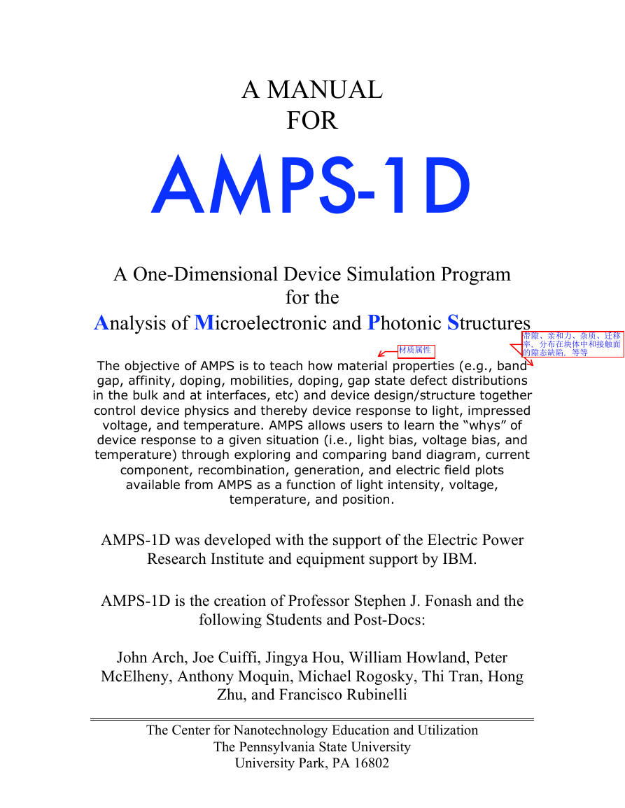
A MANUAL
FOR
AMPS-1D
A One-Dimensional Device Simulation Program
for the
Analysis of Microelectronic and Photonic Structures
The objective of AMPS is to teach how material properties (e.g., band
gap, affinity, doping, mobilities, doping, gap state defect distributions
in the bulk and at interfaces, etc) and device design/structure together
control device physics and thereby device response to light, impressed
voltage, and temperature. AMPS allows users to learn the “whys” of
device response to a given situation (i.e., light bias, voltage bias, and
temperature) through exploring and comparing band diagram, current
component, recombination, generation, and electric field plots
available from AMPS as a function of light intensity, voltage,
temperature, and position.
AMPS-1D was developed with the support of the Electric Power
Research Institute and equipment support by IBM.
AMPS-1D is the creation of Professor Stephen J. Fonash and the
following Students and Post-Docs:
John Arch, Joe Cuiffi, Jingya Hou, William Howland, Peter
McElheny, Anthony Moquin, Michael Rogosky, Thi Tran, Hong
Zhu, and Francisco Rubinelli
The Center for Nanotechnology Education and Utilization
The Pennsylvania State University
University Park, PA 16802
�
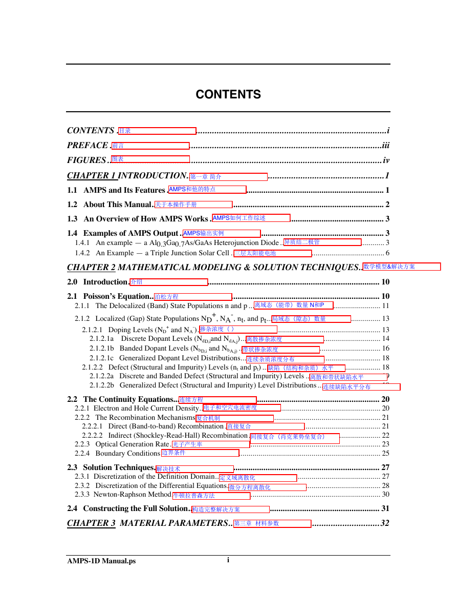
AMPS-1D Manual.psiCONTENTSCONTENTS....................................................................................................................iPREFACE.....................................................................................................................iiiFIGURES......................................................................................................................ivCHAPTER 1 INTRODUCTION.....................................................................................11.1 AMPS and Its Features.....................................................................................................11.2 About This Manual............................................................................................................21.3 An Overview of How AMPS Works.................................................................................31.4 Examples of AMPS Output...............................................................................................31.4.1 An example — a Al0.3Ga0.7As/GaAs Heterojunction Diode.....................................................31.4.2 An Example — a Triple Junction Solar Cell..............................................................................6CHAPTER 2 MATHEMATICAL MODELING & SOLUTION TECHNIQUES.........102.0 Introduction.....................................................................................................................102.1 Poisson’s Equation...........................................................................................................102.1.1 The Delocalized (Band) State Populations n and p...................................................................112.1.2 Localized (Gap) State Populations ND+, NA-, nt, and pt..........................................................132.1.2.1 Doping Levels (ND+ and NA-).............................................................................................132.1.2.1a Discrete Dopant Levels (NdD,iand NdA,j).......................................................................142.1.2.1b Banded Dopant Levels (NbD,i and NbA,j)........................................................................162.1.2.1c Generalized Dopant Level Distributions.......................................................................182.1.2.2 Defect (Structural and Impurity) Levels (nt and pt)............................................................182.1.2.2a Discrete and Banded Defect (Structural and Impurity) Levels......................................192.1.2.2b Generalized Defect (Structural and Impurity) Level Distributions................................192.2 The Continuity Equations................................................................................................202.2.1 Electron and Hole Current Density............................................................................................202.2.2 The Recombination Mechanisms..............................................................................................212.2.2.1 Direct (Band-to-band) Recombination...............................................................................212.2.2.2 Indirect (Shockley-Read-Hall) Recombination...................................................................222.2.3 Optical Generation Rate...........................................................................................................232.2.4 Boundary Conditions...............................................................................................................252.3 Solution Techniques.........................................................................................................272.3.1 Discretization of the Definition Domain....................................................................................272.3.2 Discretization of the Differential Equations..............................................................................282.3.3 Newton-Raphson Method..........................................................................................................302.4 Constructing the Full Solution.........................................................................................31CHAPTER 3 MATERIAL PARAMETERS.................................................................32�
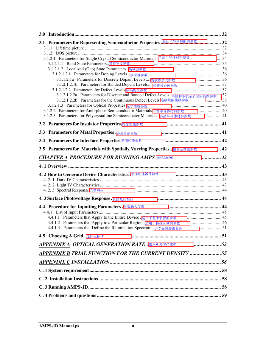
AMPS-1D Manual.psii3.0 Introduction.....................................................................................................................323.1 Parameters for Representing Semiconductor Properties................................................323.1.1 Lifetime picture.......................................................................................................................323.1.2 DOS picture.............................................................................................................................343.1.2.1 Parameters for Single Crystal Semiconductor Materials........................................................343.1.2.1.1 Band State Parameters....................................................................................................353.1.2.1.2 Localized (Gap) State Parameters...................................................................................363.1.2.1.2.1 Parameters for Doping Levels..................................................................................363.1.1.2.1a Parameters for Discrete Dopant Levels..................................................................363.1.2.1.2.1b Parameters for Banded Dopant Levels................................................................373.1.2.1.2.2 Parameters for Defect Levels....................................................................................373.1.2.1.2.2a Parameters for Discrete and Banded Defect Levels.............................................373.1.2.1.2.2b Parameters for the Continuous Defect Levels......................................................383.1.2.1.3 Parameters for Optical Properties...................................................................................403.1.2.2 Parameters for Amorphous Semiconductor Materials............................................................403.1.2.3 Parameters for Polycrystalline Semiconductor Materials........................................................413.2 Parameters for Insulator Properties................................................................................413.3 Parameters for Metal Properties.....................................................................................413.4 Parameters for Interface Properties................................................................................423.5 Parameters for Materials with Spatially Varying Properties.........................................42CHAPTER 4 PROCEDURE FOR RUNNING AMPS................................................434. 1 Overview..........................................................................................................................434. 2 How to Generate Device Characteristics..........................................................................434. 2. 1 Dark IV Characteristics..........................................................................................................434. 2. 2 Light IV Characteristics..........................................................................................................434. 2. 3 Spectral Response...................................................................................................................444. 3 Surface Photovoltage Response........................................................................................444.4 Procedure for Inputting Parameters...............................................................................444.4.1 List of Input Parameters...........................................................................................................454.4.1.1 Parameters that Apply to the Entire Device.......................................................................454.4.1.2 Parameters that Apply to a Particular Region....................................................................464.4.1.3 Parameters that Define the Illumination Spectrum.............................................................514.5 Choosing A Grid..............................................................................................................51APPENDIX A OPTICAL GENERATION RATE.......................................................53APPENDIX B TRIAL FUNCTION FOR THE CURRENT DENSITY.......................55APPENDIX C INSTALLATION..................................................................................58C. 1 System requirement.........................................................................................................58C. 2 Installation Instructions..................................................................................................58C. 3 Running AMPS-1D..........................................................................................................58C. 4 Problems and questions...................................................................................................59�
AMPS-1D Manual.psiiiPREFACEAMPS is a very general program for analyzing and designing transport in microelectronic andphotonic structures. It differs from other transport analysis programs such as PICES in a numberof ways. Among them are its ability to handle any defect and doping energy gap and specialdistribution, its incorporation of S-R-H and band-to-band recombination, its incorporation ofBoltzmann and Fermi-Dirac statistics, its ability to handle varying material properties, its verygeneral treatment of contacts, and its ability to handle transport in devices under voltage bias, lightbias, or both.This manual for AMPS-1D is intended for those using our window ‘95/NT version. We apologizein advance for the fact that this manual will get out of date but, as we are sure you understand,AMPS is a constantly growing, developing package. However, most of what is said here willremain valid and should be useful.AMPS would not exist without the support of the Electric Power Research Institute. In particularit would not exist without the encouragement, guidance, and questioning of Dr. Terry Peterson ofEPRI and without the vision of Dr. Ed DeMeo and Dr. John Crowley.Stephen FonashElectronic Materials and Processing Research LaboratoryPenn State University�
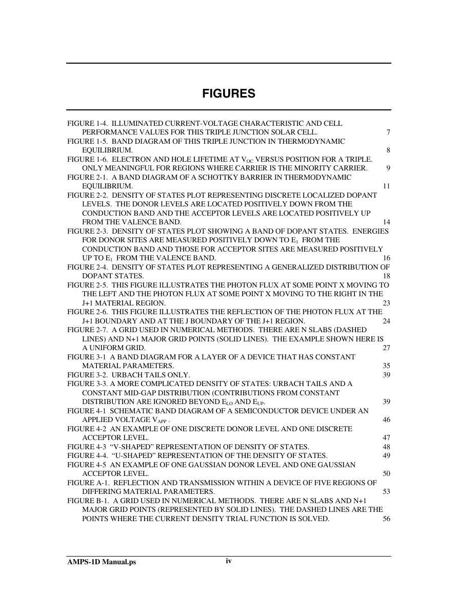
AMPS-1D Manual.psivFIGURESFIGURE 1-4. ILLUMINATED CURRENT-VOLTAGE CHARACTERISTIC AND CELLPERFORMANCE VALUES FOR THIS TRIPLE JUNCTION SOLAR CELL.7FIGURE 1-5. BAND DIAGRAM OF THIS TRIPLE JUNCTION IN THERMODYNAMICEQUILIBRIUM.8FIGURE 1-6. ELECTRON AND HOLE LIFETIME AT VOC VERSUS POSITION FOR A TRIPLE.ONLY MEANINGFUL FOR REGIONS WHERE CARRIER IS THE MINORITY CARRIER.9FIGURE 2-1. A BAND DIAGRAM OF A SCHOTTKY BARRIER IN THERMODYNAMICEQUILIBRIUM.11FIGURE 2-2. DENSITY OF STATES PLOT REPRESENTING DISCRETE LOCALIZED DOPANTLEVELS. THE DONOR LEVELS ARE LOCATED POSITIVELY DOWN FROM THECONDUCTION BAND AND THE ACCEPTOR LEVELS ARE LOCATED POSITIVELY UPFROM THE VALENCE BAND.14FIGURE 2-3. DENSITY OF STATES PLOT SHOWING A BAND OF DOPANT STATES. ENERGIESFOR DONOR SITES ARE MEASURED POSITIVELY DOWN TO E1 FROM THECONDUCTION BAND AND THOSE FOR ACCEPTOR SITES ARE MEASURED POSITIVELYUP TO E1 FROM THE VALENCE BAND.16FIGURE 2-4. DENSITY OF STATES PLOT REPRESENTING A GENERALIZED DISTRIBUTION OFDOPANT STATES.18FIGURE 2-5. THIS FIGURE ILLUSTRATES THE PHOTON FLUX AT SOME POINT X MOVING TOTHE LEFT AND THE PHOTON FLUX AT SOME POINT X MOVING TO THE RIGHT IN THEJ+1 MATERIAL REGION.23FIGURE 2-6. THIS FIGURE ILLUSTRATES THE REFLECTION OF THE PHOTON FLUX AT THEJ+1 BOUNDARY AND AT THE J BOUNDARY OF THE J+1 REGION.24FIGURE 2-7. A GRID USED IN NUMERICAL METHODS. THERE ARE N SLABS (DASHEDLINES) AND N+1 MAJOR GRID POINTS (SOLID LINES). THE EXAMPLE SHOWN HERE ISA UNIFORM GRID.27FIGURE 3-1 A BAND DIAGRAM FOR A LAYER OF A DEVICE THAT HAS CONSTANTMATERIAL PARAMETERS.35FIGURE 3-2. URBACH TAILS ONLY.39FIGURE 3-3. A MORE COMPLICATED DENSITY OF STATES: URBACH TAILS AND ACONSTANT MID-GAP DISTRIBUTION (CONTRIBUTIONS FROM CONSTANTDISTRIBUTION ARE IGNORED BEYOND ELO AND EUP.39FIGURE 4-1 SCHEMATIC BAND DIAGRAM OF A SEMICONDUCTOR DEVICE UNDER ANAPPLIED VOLTAGE VAPP .46FIGURE 4-2 AN EXAMPLE OF ONE DISCRETE DONOR LEVEL AND ONE DISCRETEACCEPTOR LEVEL.47FIGURE 4-3 “V-SHAPED” REPRESENTATION OF DENSITY OF STATES.48FIGURE 4-4. “U-SHAPED” REPRESENTATION OF THE DENSITY OF STATES.49FIGURE 4-5 AN EXAMPLE OF ONE GAUSSIAN DONOR LEVEL AND ONE GAUSSIANACCEPTOR LEVEL.50FIGURE A-1. REFLECTION AND TRANSMISSION WITHIN A DEVICE OF FIVE REGIONS OFDIFFERING MATERIAL PARAMETERS.53FIGURE B-1. A GRID USED IN NUMERICAL METHODS. THERE ARE N SLABS AND N+1MAJOR GRID POINTS (REPRESENTED BY SOLID LINES). THE DASHED LINES ARE THEPOINTS WHERE THE CURRENT DENSITY TRIAL FUNCTION IS SOLVED.56�
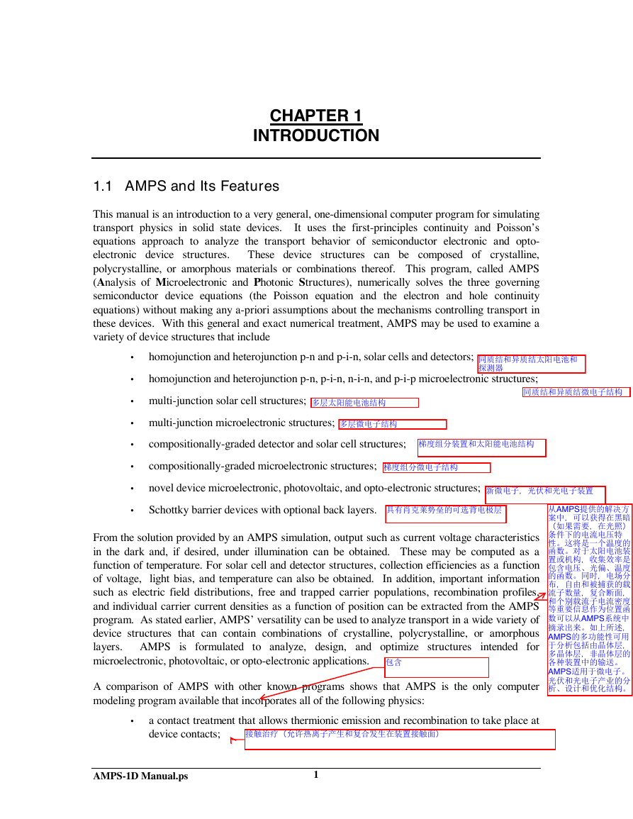
AMPS-1D Manual.ps1CHAPTER 1INTRODUCTION1.1 AMPS and Its FeaturesThis manual is an introduction to a very general, one-dimensional computer program for simulatingtransport physics in solid state devices. It uses the first-principles continuity and Poisson’sequations approach to analyze the transport behavior of semiconductor electronic and opto-electronic device structures. These device structures can be composed of crystalline,polycrystalline, or amorphous materials or combinations thereof. This program, called AMPS(Analysis of Microelectronic and Photonic Structures), numerically solves the three governingsemiconductor device equations (the Poisson equation and the electron and hole continuityequations) without making any a-priori assumptions about the mechanisms controlling transport inthese devices. With this general and exact numerical treatment, AMPS may be used to examine avariety of device structures that include• homojunction and heterojunction p-n and p-i-n, solar cells and detectors;• homojunction and heterojunction p-n, p-i-n, n-i-n, and p-i-p microelectronic structures;• multi-junction solar cell structures;• multi-junction microelectronic structures;• compositionally-graded detector and solar cell structures;• compositionally-graded microelectronic structures;• novel device microelectronic, photovoltaic, and opto-electronic structures;• Schottky barrier devices with optional back layers.From the solution provided by an AMPS simulation, output such as current voltage characteristicsin the dark and, if desired, under illumination can be obtained. These may be computed as afunction of temperature. For solar cell and detector structures, collection efficiencies as a functionof voltage, light bias, and temperature can also be obtained. In addition, important informationsuch as electric field distributions, free and trapped carrier populations, recombination profiles,and individual carrier current densities as a function of position can be extracted from the AMPSprogram. As stated earlier, AMPS’ versatility can be used to analyze transport in a wide variety ofdevice structures that can contain combinations of crystalline, polycrystalline, or amorphouslayers. AMPS is formulated to analyze, design, and optimize structures intended formicroelectronic, photovoltaic, or opto-electronic applications.A comparison of AMPS with other known programs shows that AMPS is the only computermodeling program available that incorporates all of the following physics:• a contact treatment that allows thermionic emission and recombination to take place atdevice contacts;�
AMPS-1D Manual.ps2• a very generalized gap state model that can fit any density of states distribution in thebulk or at an interface;• both band-to-band and Shockley-Read-Hall recombination;• a recombination model that computes Shockley-Read-Hall recombination trafficthrough any inputted general gap state distribution instead of the often-used singlerecombination level approach;• full Fermi-Dirac, and not just Boltzmann, statistics;• gap state populations computed with actual-temperature statistics rather than the oftenused T=0K approach;• a trapped charge model that accounts for charge in any inputted general gap statedistribution;• a gap state model that allows capture cross-sections to vary with energy;• gap state distributions whose properties can vary with position;• carrier mobility that can vary with position;• electron and hole affinities that can vary with position;• mobility gaps that can differ from optical gaps;• the ability to calculate device characteristics as a function of temperature in bothforward and reverse bias as well as with or without illumination;• the ability to analyze device structures fabricated using single crystal, polycrystalline,or amorphous materials or all three.1.2 About This ManualThis manual assumes the user has completed an introductory course in semiconductor devicephysics and is familiar with mathematical concepts such as Poisson’s equation and the continuityequations. A working knowledge of numerical methods is helpful, but not actually required forworking with the AMPS program. This manual explains the approach used in AMPS for• modeling of hole and electron transport, including a discussion of the basic equationsand solution techniques (Chapter 2);• parameterizing material properties (Chapter 3)• semiconductor materials• insulators• metals• interfaces• materials with position dependent properties;�
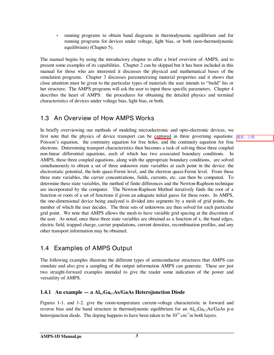
AMPS-1D Manual.ps3• running programs to obtain band diagrams in thermodynamic equilibrium and forrunning programs for devices under voltage, light bias, or both (non-thermodynamicequilibrium) (Chapter 5).The manual begins by using the introductory chapter to offer a brief overview of AMPS, and topresent some examples of its capabilities. Chapter 2 can be skipped but it has been included in thismanual for those who are interested it discusses the physical and mathematical bases of thesimulation programs. Chapter 3 discusses parameterizing material properties and it shows thatclose attention must be given to the particular types of materials the user intends to “build” his orher structure. The AMPS programs will ask the user to input these specific parameters. Chapter 4describes the heart of AMPS: the procedures for obtaining the detailed physics and terminalcharacteristics of devices under voltage bias, light bias, or both.1.3 An Overview of How AMPS WorksIn briefly overviewing our methods of modeling microelectronic and opto-electronic devices, wefirst note that the physics of device transport can be captured in three governing equations:Poisson’s equation, the continuity equation for free holes, and the continuity equation for freeelectrons. Determining transport characteristics then becomes a task of solving these three couplednon-linear differential equations, each of which has two associated boundary conditions. InAMPS, these three coupled equations, along with the appropriate boundary conditions, are solvedsimultaneously to obtain a set of three unknown state variables at each point in the device: theelectrostatic potential, the hole quasi-Fermi level, and the electron quasi-Fermi level. From thesethree state variables, the carrier concentrations, fields, currents, etc. can then be computed. Todetermine these state variables, the method of finite differences and the Newton-Raphson techniqueare incorporated by the computer. The Newton-Raphson Method iteratively finds the root of afunction or roots of a set of functions if given an adequate initial guess for these roots. In AMPS,the one-dimensional device being analyzed is divided into segments by a mesh of grid points, thenumber of which the user decides. The three sets of unknowns are then solved for each particulargrid point. We note that AMPS allows the mesh to have variable grid spacing at the discretion ofthe user. As noted, once these three state variables are obtained as a function of x, the band edges,electric field, trapped charge, carrier populations, current densities, recombination profiles, and anyother transport information may be obtained.1.4 Examples of AMPS OutputThe following examples illustrate the different types of semiconductor structures that AMPS cansimulate and also give a sampling of the output information AMPS can generate. These are justtwo straight-forward examples intended to give the reader some indication of the power andversatility of AMPS.1.4.1 An example — a Al0.3Ga0.7As/GaAs Heterojunction DiodeFigures 1-1. and 1-2. give the room-temperature current-voltage characteristic in forward andreverse bias and the band structure in thermodynamic equilibrium for an Al0.3Ga0.7As/GaAs p-nheterojunction diode. The doping happens to have been taken to be 1016 cm-3 in both layers.�




 2023年江西萍乡中考道德与法治真题及答案.doc
 2012年重庆南川中考生物真题及答案.doc
 2013年江西师范大学地理学综合及文艺理论基础考研真题.doc
 2020年四川甘孜小升初语文真题及答案I卷.doc
 2020年注册岩土工程师专业基础考试真题及答案.doc
 2023-2024学年福建省厦门市九年级上学期数学月考试题及答案.doc
 2021-2022学年辽宁省沈阳市大东区九年级上学期语文期末试题及答案.doc
 2022-2023学年北京东城区初三第一学期物理期末试卷及答案.doc
 2018上半年江西教师资格初中地理学科知识与教学能力真题及答案.doc
 2012年河北国家公务员申论考试真题及答案-省级.doc
 2020-2021学年江苏省扬州市江都区邵樊片九年级上学期数学第一次质量检测试题及答案.doc
 2022下半年黑龙江教师资格证中学综合素质真题及答案.doc