INTEGRATED CIRCUITS
PCA9554/PCA9554A
8-bit I2C and SMBus I/O port with interrupt
Product data
Supersedes data of 2002 May 13
2002 Jul 26
Ps
onos
�
Philips Semiconductors
Product data
8-bit I2C and SMBus I/O port with interrupt
PCA9554/PCA9554A
DESCRIPTION
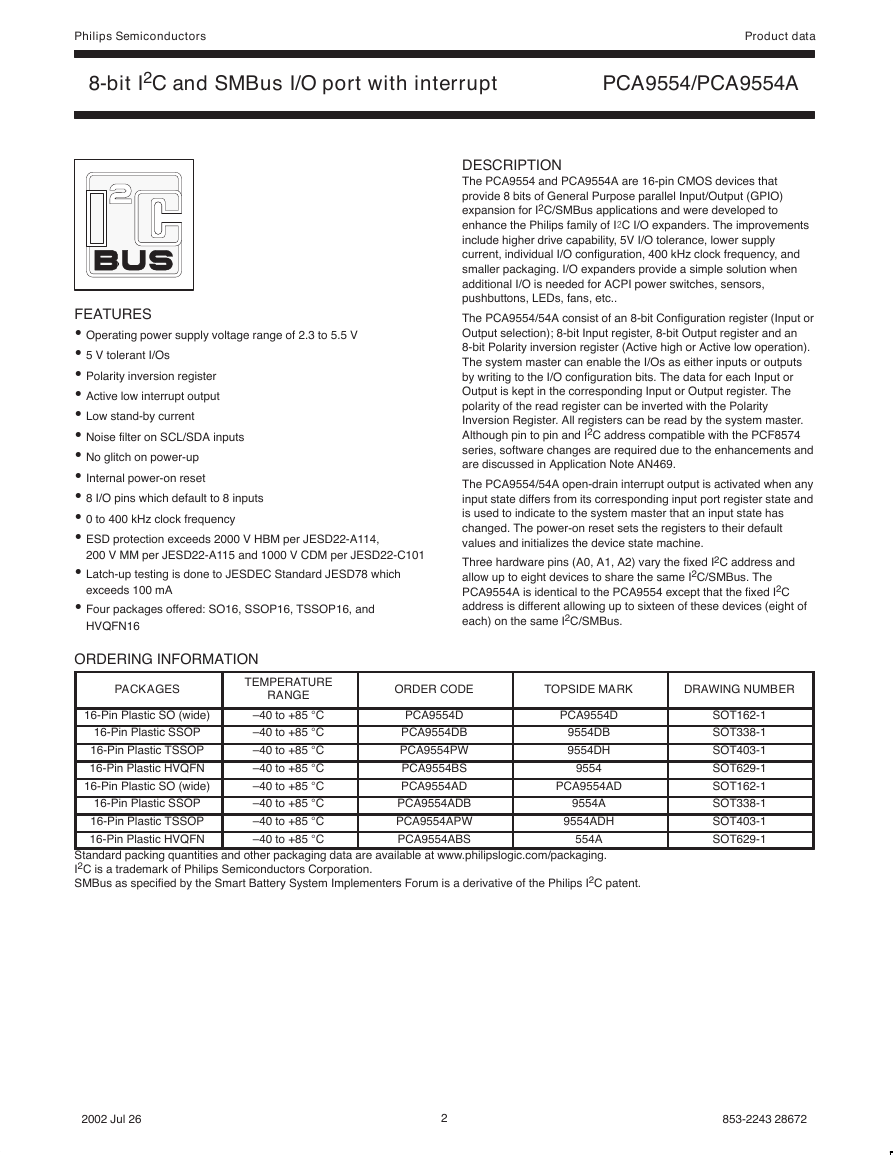
The PCA9554 and PCA9554A are 16-pin CMOS devices that
provide 8 bits of General Purpose parallel Input/Output (GPIO)
expansion for I2C/SMBus applications and were developed to
enhance the Philips family of I@C I/O expanders. The improvements
include higher drive capability, 5V I/O tolerance, lower supply
current, individual I/O configuration, 400 kHz clock frequency, and
smaller packaging. I/O expanders provide a simple solution when
additional I/O is needed for ACPI power switches, sensors,
pushbuttons, LEDs, fans, etc..
The PCA9554/54A consist of an 8-bit Configuration register (Input or
Output selection); 8-bit Input register, 8-bit Output register and an
8-bit Polarity inversion register (Active high or Active low operation).
The system master can enable the I/Os as either inputs or outputs
by writing to the I/O configuration bits. The data for each Input or
Output is kept in the corresponding Input or Output register. The
polarity of the read register can be inverted with the Polarity
Inversion Register. All registers can be read by the system master.
Although pin to pin and I2C address compatible with the PCF8574
series, software changes are required due to the enhancements and
are discussed in Application Note AN469.
The PCA9554/54A open-drain interrupt output is activated when any
input state differs from its corresponding input port register state and
is used to indicate to the system master that an input state has
changed. The power-on reset sets the registers to their default
values and initializes the device state machine.
Three hardware pins (A0, A1, A2) vary the fixed I2C address and
allow up to eight devices to share the same I2C/SMBus. The
PCA9554A is identical to the PCA9554 except that the fixed I2C
address is different allowing up to sixteen of these devices (eight of
each) on the same I2C/SMBus.
FEATURES
• Operating power supply voltage range of 2.3 to 5.5 V
• 5 V tolerant I/Os
• Polarity inversion register
• Active low interrupt output
• Low stand-by current
• Noise filter on SCL/SDA inputs
• No glitch on power-up
• Internal power-on reset
• 8 I/O pins which default to 8 inputs
• 0 to 400 kHz clock frequency
• ESD protection exceeds 2000 V HBM per JESD22-A114,
200 V MM per JESD22-A115 and 1000 V CDM per JESD22-C101
• Latch-up testing is done to JESDEC Standard JESD78 which
exceeds 100 mA
• Four packages offered: SO16, SSOP16, TSSOP16, and
HVQFN16
ORDERING INFORMATION
TEMPERATURE
RANGE
ORDER CODE
TOPSIDE MARK
DRAWING NUMBER
PCA9554D
9554DB
9554DH
9554
PCA9554AD
9554A
9554ADH
SOT162-1
SOT338-1
SOT403-1
SOT629-1
SOT162-1
SOT338-1
SOT403-1
SOT629-1
PACKAGES
16-Pin Plastic SO (wide)
16-Pin Plastic SSOP
16-Pin Plastic TSSOP
16-Pin Plastic HVQFN
16-Pin Plastic SO (wide)
16-Pin Plastic SSOP
16-Pin Plastic TSSOP
16-Pin Plastic HVQFN
–40 to +85 °C
–40 to +85 °C
–40 to +85 °C
–40 to +85 °C
–40 to +85 °C
–40 to +85 °C
–40 to +85 °C
–40 to +85 °C
PCA9554D
PCA9554DB
PCA9554PW
PCA9554BS
PCA9554AD
PCA9554ADB
PCA9554APW
PCA9554ABS
554A
Standard packing quantities and other packaging data are available at www.philipslogic.com/packaging.
I2C is a trademark of Philips Semiconductors Corporation.
SMBus as specified by the Smart Battery System Implementers Forum is a derivative of the Philips I2C patent.
2002 Jul 26
2
853-2243 28672
�
Philips Semiconductors
Product data
8-bit I2C and SMBus I/O port with interrupt
PCA9554/PCA9554A
PIN CONFIGURATION — SO, SSOP, TSSOP
PIN CONFIGURATION — HVQFN
A0
A1
A2
I/O0
I/O1
I/O2
I/O3
VSS
1
2
3
4
5
6
7
8
16
VDD
15
SDA
14
13
SCL
INT
12
I/O7
11
10
9
I/O6
I/O5
I/O4
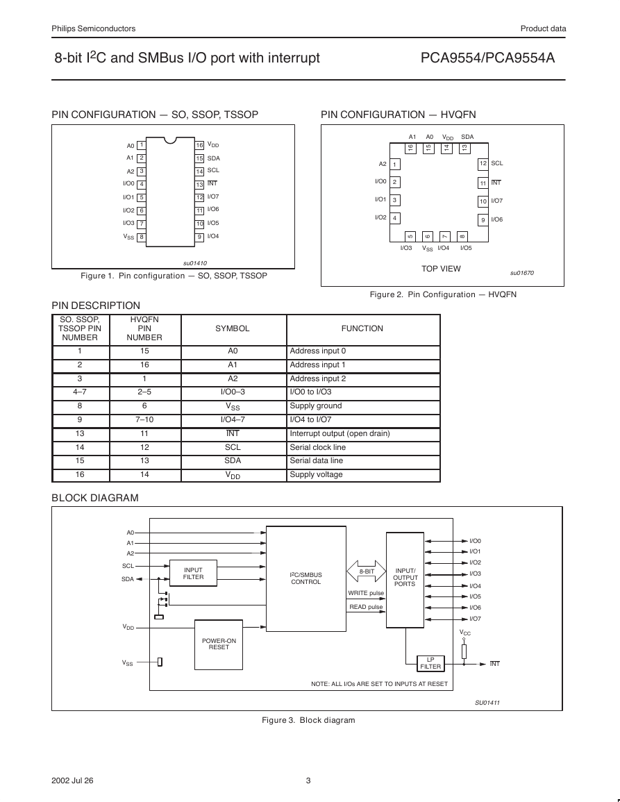
Figure 1. Pin configuration — SO, SSOP, TSSOP
su01410
PIN DESCRIPTION
A1
6
1
A0
5
1
VDD
4
1
SDA
3
1
A2
I/O0
I/O1
I/O2
1
2
3
4
12
SCL
11
INT
10
I/O7
9
I/O6
5 6 7 8
I/O3
VSS
I/O4
I/O5
TOP VIEW
su01670
Figure 2. Pin Configuration — HVQFN
SO. SSOP,
TSSOP PIN
NUMBER
1
2
3
4–7
8
9
13
14
15
16
HVQFN
PIN
NUMBER
15
16
1
2–5
6
7–10
11
12
13
14
SYMBOL
FUNCTION
A0
A1
A2
I/O0–3
VSS
I/O4–7
INT
SCL
SDA
VDD
Address input 0
Address input 1
Address input 2
I/O0 to I/O3
Supply ground
I/O4 to I/O7
Interrupt output (open drain)
Serial clock line
Serial data line
Supply voltage
BLOCK DIAGRAM
A0
A1
A2
SCL
SDA
VDD
VSS
INPUT
FILTER
I2C/SMBUS
CONTROL
8-BIT
INPUT/
OUTPUT
PORTS
WRITE pulse
READ pulse
POWER-ON
RESET
I/O0
I/O1
I/O2
I/O3
I/O4
I/O5
I/O6
I/O7
VCC
LP
FILTER
INT
NOTE: ALL I/Os ARE SET TO INPUTS AT RESET
SU01411
Figure 3. Block diagram
2002 Jul 26
3
�
Philips Semiconductors
Product data
8-bit I2C and SMBus I/O port with interrupt
PCA9554/PCA9554A
Register 2 – Polarity Inversion Register
bit
default
N7
0
N6
0
N5
0
N4
0
N3
0
N2
0
N1
0
N0
0
This register allows the user to invert the polarity of the Input Port
Register data. If a bit in this register is set (written with ‘1’), the
corresponding Input Port data is inverted. If a bit in this register is
cleared (written with a ‘0’), the Input Port data polarity is retained.
Register 3 – Configuration Register
bit
default
C7
1
C6
1
C5
1
C4
1
C3
1
C2
1
C1
1
C0
1
This register configures the directions of the I/O pins. If a bit in this
register is set, the corresponding port pin is enabled as an input with
high impedance output driver. If a bit in this register is cleared, the
corresponding port pin is enabled as an output. At reset, the I/Os are
configured as inputs with a weak pull-up to VDD.
Power-on Reset
When power is applied to VDD, an internal power-on reset holds the
PCA9554 in a reset state until VDD has reached VPOR. At that point,
the reset condition is released and the PCA9554 registers and state
machine will initialize to their default states.
Interrupt Output
The open-drain interrupt output is activated when one of the port
pins change state and the pin is configured as an input. The
interrupt is deactivated when the input returns to its previous state or
the input port register is read.
Note that changing an I/O from an output to an input may cause a
false interrupt to occur if the state of the pin does not match the
contents of the input port register.
REGISTERS
Command Byte
Command
Protocol
Function
0
1
2
3
Read byte
Input port register
Read/write byte
Output port register
Read/write byte
Polarity inversion register
Read/write byte
Configuration register
The command byte is the first byte to follow the address byte during
a write transmission. It is used as a pointer to determine which of the
following registers will be written or read.
Register 0 – Input Port Register
I3
bit
I6
I7
I5
I4
default
1
1
1
1
1
I2
1
I1
1
I0
1
This register is a read only port. It reflects the incoming logic levels
of the pins, regardless of whether the pin is defined as an input or an
output by Register 3. Writes to this register have no effect.
Register 1 – Output Port Register
O3
O7
O6
O5
O4
bit
default
1
1
1
1
1
O2
1
O1
1
O0
1
This register reflects the outgoing logic levels of the pins defined as
outputs by Register 3. Bit values in this register have no effect on
pins defined as inputs. Reads from this register return the value that
is in the flip-flop controlling the output selection, NOT the actual pin
value.
2002 Jul 26
4
�
Philips Semiconductors
Product data
8-bit I2C and SMBus I/O port with interrupt
PCA9554/PCA9554A
SIMPLIFIED SCHEMATIC OF I/O0 TO I/O7
CONFIGURATION
REGISTER
D
Q
FF
CK
Q
D
Q
FF
CK
Q
OUTPUT
PORT
REGISTER
DATA FROM
SHIFT REGISTER
DATA FROM
SHIFT REGISTER
WRITE
CONFIGURATION
PULSE
WRITE PULSE
READ PULSE
DATA FROM
SHIFT REGISTER
WRITE
POLARITY
PULSE
Q1
100 kW
Q2
INPUT PORT
REGISTER
D
Q
FF
CK
Q
D
Q
FF
CK
Q
POLARITY
INVERSION
REGISTER
OUTPUT PORT
REGISTER DATA
VDD
I/O0 TO I/O7
VSS
INPUT PORT
REGISTER DATA
TO INT
POLARITY
REGISTER DATA
SU01472
NOTE: At Power-on Reset, all registers return to default values.
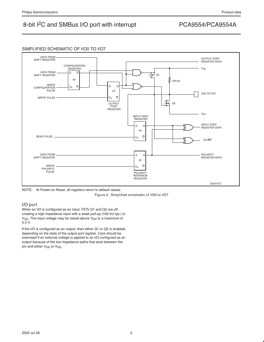
Figure 4. Simplified schematic of I/O0 to I/O7
I/O port
When an I/O is configured as an input, FETs Q1 and Q2 are off,
creating a high impedance input with a weak pull-up (100 kW
VDD. The input voltage may be raised above VDD to a maximum of
5.5 V.
typ.) to
If the I/O is configured as an output, then either Q1 or Q2 is enabled,
depending on the state of the output port register. Care should be
exercised if an external voltage is applied to an I/O configured as an
output because of the low impedance paths that exist between the
pin and either VDD or VSS.
2002 Jul 26
5
�
Philips Semiconductors
Product data
8-bit I2C and SMBus I/O port with interrupt
PCA9554/PCA9554A
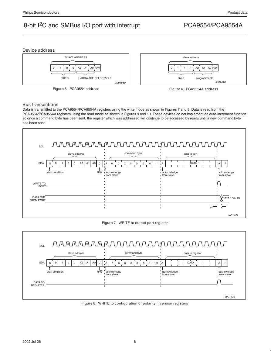
Device address
SLAVE ADDRESS
slave address
0
1
0
0
A2 A1 A0
R/W
0
1
1
1
A2 A1 A0
R/W
FIXED
HARDWARE SELECTABLE
su01669
Figure 5. PCA9554 address
fixed
programmable
su01418
Figure 6. PCA9554A address
Bus transactions
Data is transmitted to the PCA9554/PCA9554A registers using the write mode as shown in Figures 7 and 8. Data is read from the
PCA9554/PCA9554A registers using the read mode as shown in Figures 9 and 10. These devices do not implement an auto-increment function
so once a command byte has been sent, the register which was addressed will continue to be accessed by reads until a new command byte
has been sent.
SCL
1
2
3
4
5
6
7
8
9
slave address
command byte
data to port
SDA
S
0
1
0
0
A2 A1 A0
0
A
0
0
0
0
0
0
0
1
A
DATA 1
A
P
start condition
R/W acknowledge
from slave
acknowledge
from slave
acknowledge
from slave
WRITE TO
PORT
DATA OUT
FROM PORT
Figure 7. WRITE to output port register
tpv
DATA 1 VALID
su01421
SCL
1
2
3
4
5
6
7
8
9
slave address
command byte
data to register
SDA
S
0
1
0
0
A2 A1 A0
0
A
0
0
0
0
0
0
1
1/0
A
DATA
A
P
start condition
R/W acknowledge
from slave
acknowledge
from slave
acknowledge
from slave
DATA TO
REGISTER
Figure 8. WRITE to configuration or polarity inversion registers
su01422
2002 Jul 26
6
�
Philips Semiconductors
Product data
8-bit I2C and SMBus I/O port with interrupt
PCA9554/PCA9554A
slave address
acknowledge
from slave
acknowledge
from slave
slave address
acknowledge
from slave
data from register
acknowledge
from master
S
0
1
0
0 A2 A1 A0
0
A
COMMAND BYTE
A
S
0
1
0
0 A2 A1 A0
1
A
R/W
R/W
DATA
first byte
A
at this moment master-transmitter
becomes master-receiver and
slave-receiver becomes
slave-transmitter
data from register
no acknowledge
from master
DATA
last byte
NA
P
su01424
Figure 9. READ from register
SCL
1
2
3
4
5
6
7
8
9
slave address
data from port
data from port
SDA
S
0
1
0
0
A2 A1 A0
1
A
DATA 1
A
DATA 4
NA
P
start condition
R/W acknowledge
from slave
acknowledge
from master
no acknowledge
from master
stop
condition
READ FROM
PORT
DATA INTO
PORT
INT
tiv
DATA 2
DATA 3
DATA 4
tps
tph
tir
su01465
NOTES:
1. This figure assumes the command byte has previously been programmed with 00h.
2. Transfer of data can be stopped at any moment by a stop condition.
Figure 10. READ input port register
2002 Jul 26
7
�
Philips Semiconductors
Product data
8-bit I2C and SMBus I/O port with interrupt
PCA9554/PCA9554A
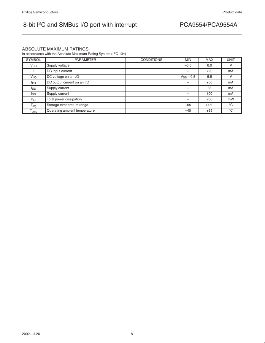
ABSOLUTE MAXIMUM RATINGS
In accordance with the Absolute Maximum Rating System (IEC 134)
SYMBOL
PARAMETER
CONDITIONS
VDD
II
VI/O
II/O
IDD
ISS
Ptot
Tstg
Tamb
Supply voltage
DC input current
DC voltage on an I/O
DC output current on an I/O
Supply current
Supply current
Total power dissipation
Storage temperature range
Operating ambient temperature
MIN
–0.5
—
VSS – 0.5
—
—
—
—
–65
–40
MAX
6.0
±20
5.5
±50
85
100
200
+150
+85
UNIT
V
mA
V
mA
mA
mA
mW
°C
°C
2002 Jul 26
8
�




 2023年江西萍乡中考道德与法治真题及答案.doc
 2012年重庆南川中考生物真题及答案.doc
 2013年江西师范大学地理学综合及文艺理论基础考研真题.doc
 2020年四川甘孜小升初语文真题及答案I卷.doc
 2020年注册岩土工程师专业基础考试真题及答案.doc
 2023-2024学年福建省厦门市九年级上学期数学月考试题及答案.doc
 2021-2022学年辽宁省沈阳市大东区九年级上学期语文期末试题及答案.doc
 2022-2023学年北京东城区初三第一学期物理期末试卷及答案.doc
 2018上半年江西教师资格初中地理学科知识与教学能力真题及答案.doc
 2012年河北国家公务员申论考试真题及答案-省级.doc
 2020-2021学年江苏省扬州市江都区邵樊片九年级上学期数学第一次质量检测试题及答案.doc
 2022下半年黑龙江教师资格证中学综合素质真题及答案.doc