�
ANALYSIS AND DESIGN
OF ANALOG INTEGRATED
CIRCUITS
Fourth Edition
PAUL R. GRAY
University of California, Berkeley
PAUL J. HURST
University of California, Davis
STEPHEN H. LEWIS
University of California, Davis
ROBERT G. MEYER
University of California, Berkeley
JOHN WlLEY & SONS, INC.
New York / Chichester / Weinheim / Brisbane /Singapore / Toronto
-7 C L-,
ACQUISITIONS EDITOR
EDITORIAL ASSISTANT
William Zobrist
Susannah Barr
SENIOR MARKETING MANAGER
Katherine Hepburn
PRODUCTION SERVICES MANAGER
Jeanine Furino
PRODUCTION EDITOR
DESIGN DIRECTOR
Sandra Russell
Madelyn Lesure
PRODUCTION MANAGEMENT SERVICES
Publication Services, Inc.
Cover courtesy of Dr. Kenneth C. Dyer and Melgar Photography.
This book was set in 10i12 Times Roman by Publication Services, Inc. and printed and bound by
Hamilton Printing Company. The cover was printed by Lehigh Press, Inc.
This book was printed on acid-free paper. @
Copyright 2001 O John Wiley & Sons, Inc. All rights reserved.
No part of this publication may be reproduced, stored in a retrieval system or transmitted
in any form or by any means, electronic, mechanical, photocopying, recording, scanning
or otherwise, except as permitted under Sections 107 or 108 of the 1976 United States
Copyright Act, without either the prior written permission of the Publisher, or
authorization through payment of the appropriate per-copy fee to the Copyright
Clearance Center, 222 Rosewood Drive, Danvers, MA 01923, (978) 750-8400, fax
(978) 750-4470. Requests to the Publisher for permission should be addressed to the
Permissions Department, John Wiley & Sons, Inc., 605 Third Avenue, New York, NY
10158-0012, (212) 850-6011, fax (212) 850-6008, E-mail: PERMREQ@WILEY.COM.
To order books or for customer service please call 1-800-CALL-WILEY (255-5945).
Library of Congress Cataloging-in-Publication Data
Analysis and design of analog integrated circuits 1 Paul R. Gray. . .[et al.]. - 4th ed.
p. cm.
lncludes bibliographical references and index.
ISBN 0-471-32 168-0 (cloth: alk. paper)
1. Linear integrated circuits-Computer-aided design. 2. Metal oxide
semiconductors-Computer-aided design. 3. Bipolar transistors-Computer-aided design.
I. Gray, Paul R., 1942-
TK7874.A588 2000
621.38154~21
Printed in the United States of America
1 0 9 8 7 6 5 4 3 2 1
00-043583
�
Preface
In the 23 years since the publication of the first edition of this book, the field df analog
integrated circuits has developed and matured. The initial groundwork was laid in bipolar
technology, followed by a rapid evolution of MOS analog integrated circuits. Further-
more, BiCMOS technology (incorporating both bipolar and CMOS devices on one chip)
has emerged as a serious contender to the original technologies. A key issue is that CMOS
technologies have become dominant in building digital circuits because CMOS digital
circuits are smaller and dissipate less power than their bipolar counterparts. To reduce
system cost and power dissipation, analog and digital circuits are now often integrated
together, providing a strong economic incentive to use CMOS-compatible analog circuits.
As a result, an important question in many applications is whether to use pure CMOS or a
BiCMOS technology. Although somewhat more expensive to fabricate, BiCMOS allows
the designer to use both bipolar and MOS devices to their best advantage, and also al-
lows innovative combinations of the characteristics of both devices. In addition, BiCMOS
can reduce the design time by allowing direct use of many existing cells in realizing a
given analog circuit function. On the other hand, the main advantage of pure CMOS is
that it offers the lowest overall cost. Twenty years ago, CMOS technologies were only fast
enough to support applications at audio frequencies. However, the continuing reduction of
the minimum feature size in integrated-circuit (IC) technologies has greatly increased the
maximum operating frequencies, and CMOS technologies have become fast enough for
many new applications as a result. For example, the required bandwidth in video appli-
cations is about 4 MHz, requiring bipolar technologies as recently as 15 years ago. Now,
however, CMOS can easily accommodate the required bandwidth for video and is even
being used for radio-frequency applications.
In this fourth edition, we have combined the consideration of MOS and bipolar cir-
cuits into a unified treatment that also includes MOS-bipolar connections made possible
by BiCMOS technology. We have written this edition so that instructors can easily se-
lect topics related to only CMOS circuits, only bipolar circuits, or a combination of both.
We believe that it has become increasingly important for the analog circuit designer to
have a thorough appreciation of the similarities and differences between MOS and bipolar
devices, and to be able to design with either one where this is appropriate.
Since the SPICE computer analysis program is now readily available to virtually
all electrical engineering students and professionals, we have included extensive use of ,
SPICE in this edition, particularly as an integral part of many problems. We have used
computer analysis as it is most commonly employed in the engineering design process-
both as a more accurate check on hand calculations, and also as a tool to examine complex
circuit behavior beyond the scope of hand analysis. In the problem sets, we have also in-
cluded a number of open-ended design problems to expose the reader to real-world situa-
tions where a whole range of circuit solutions may be found to satisfy a given performance
specification.
This book is intended to be useful both as a text for students and as a reference book
for practicing engineers. For class use, each chapter includes many worked problems; the
problem sets at the end of each chapter illustrate the practical applications of the material
in the text. All the authors have had extensive industrial experience in IC design as well
�
viii Preface
as in the teaching of courses on this subject, and this experience is reflected in the choice
of text material and in the problem sets.
Although this book is concerned largely with the analysis and design of ICs, a consid-
erable amount of material is also included on applications. In practice, these two subjects
are closely linked, and a knowledge of both is essential for designers and users of ICs.
The latter compose the larger group by far, and we believe that a working knowledge of
IC design is a great advantage to an IC user. This is particularly apparent when the user
mdst choose from among a number of competing designs to satisfy a particular need. An
understanding of the IC structure is then useful in evaluating the relative desirability of the
different designs under extremes of environment or in the presence of variations in supply
voltage. In addition, the IC user is in a much better position to interpret a manufacturer's
data if he or she has a working knowledge of the internal operation of the integrated circuit.
The contents of this book stem largely from courses on analog integrated circuits given
at the University of California at the Berkeley and Davis campuses. The courses are un-
dergraduate electives and first-year graduate courses. The book is structured so that it
can be used as the basic text for a sequence of such courses. The more advanced mate-
rial is found at the end of each chapter or in an appendix so that a first course in analog
integrated circuits can omit this material without loss of continuity. An outline of each
chapter is given below together with suggestions for material to be covered in such a first
course. It is assumed that the course consists of three hours of lecture per week over a
15-week semester and that the students have a working knowledge of Laplace transforms
and frequency-domain circuit analysis. It is also assumed that the students have had an
introductory course in electronics so that they are familiar with the principles of transistor
operation and with the functioning of simple analog circuits. Unless otherwise stated, each
chapter requires three to four lecture hours to cover.
Chapter 1 contains a summary of bipolar transistor and MOS transistor device physics.
We suggest spending one week on selected topics from this chapter, the choice of topics
depending on the background of the students. The material of Chapters 1 and 2 is quite
important in IC design because there is significant interaction between circuit and device
design, as will be seen in later chapters. A thorough understanding of the influence of
device fabrication on device characteristics is essential.
Chapter 2 is concerned with the technology of IC fabrication and is largely descriptive.
One lecture on this material should suffice if the students are assigned to read the chapter.
Chapter 3 deals with the characteristics of elementary transistor connections. The ma-
terial on one-transistor amplifiers should be a review for students at the senior and gradu-
ate levels and can be assigned as reading. The section on two-transistor amplifiers can be
covered in about three hours, with greatest emphasis on differential pairs. The material on
device mismatch effects in differential amplifiers can be covered to the extent that time
allows.
In Chapter 4, the important topics of current mirrors and active loads are considered.
These configurations are basic building blocks in modern analog IC design, and this ma-
terial should be covered in full, with the exception of the material on band-gap references
and the material in the appendices.
Chapter 5 is concerned with output stages and methods of delivering output power to
a load. Integrated-circuit realizations of Class A, Class B, and Class AB output stages are
described, as well as methods of output-stage protection. A selection of topics from this
chapter should be covered.
Chapter 6 deals with the design of operational amplifiers (op amps). Illustrative exam-
ples of dc and ac analysis in both MOS and bipolar op amps are performed in detail, and
the limitations of the basic op amps are described. The design of op amps with improved
�
characteristics in both MOS and bipolar technologies is considered. This key chapter on
amplifier design requires at least six hours.
Preface
ix
In Chapter 7, the frequency response of amplifiers is considered. The zero-value time-
constant technique is introduced for the calculations of the -3-dB frequency of complex
circuits. The material of this chapter should be considered in full.
Chapter 8 describes the analysis of feedback circuits. Two different types of analysis
are presented: two-port and return-ratio analyses. Either approach should be covered in
full with the section on voltage regulators assigned as reading.
Chapter 9 deals with the frequency response and stability of feedback circuits and
should be covered up to the section on root locus. Time may not pennit a detailed discussion
of root locus, but some introduction to this topic can be given.
In a 15-week semester, coverage of the above material leaves about two weeks for
Chapters 10, 11, and 12. A selection of topics from these chapters can be chosen as follows.
Chapter 10 deals with nonlinear analog circuits, and portions of this chapter up to Section
10.3 could be covered in a first course. Chapter 11 is a comprehensive treatment of noise
in integrated circuits, and material up to and including Section 11.4 is suitable. Chapter 12
describes fully differential operational amplifiers and common-mode feedback and may
be best suited for a second course.
We are grateful to the following colleagues for their suggestions for andlor eval-
uation of this edition: R. Jacob Baker, Bemhard E. Boser, A. Paul Brokaw, John N.
Churchill, David W. Cline, Ozan E. Erdogan, John W. Fattaruso, Weinan Gao, Edwin W.
Greeneich, Alex Gros-Balthazard, Tiinde Gyurics, Ward J. Helms, Timothy H. Hu, Shafiq
M. Jamal, John P. Keane, Haideh Khorramabadi, Pak-Kim Lau, Thomas W. Matthews,
Krishnaswamy Nagaraj, Khalil Najafi, Borivoje NikoliC, Robert A. Pease, Lawrence T.
Pileggi, Edgar Shnchez-Sinencio, Bang-Sup Song, Richard R. Spencer, Eric J. Swanson,
Andrew Y. J. Szeto, Yannis P. Tsividis, Srikanth Vaidianathan, T. R. Viswanathan, Chomg-
Kuang Wang, and Dong Wang. We are also grateful to Kenneth C. Dyer for allowing us to
use on the cover of this book a die photograph of an integrated circuit he designed and to
Zoe Marlowe for her assistance with word processing. Finally, we would like to thank the
people at Wiley and Publication Services for their efforts in producing this fourth edition.
The material in this book has been greatly influenced by our association with Donald
0. Pederson, and we acknowledge his contributions.
Berkeley and Davis, CA, 2001
Paul R. Gray
Paul J. Hurst
Stephen H. Lewis
Robert G. Meyer
�
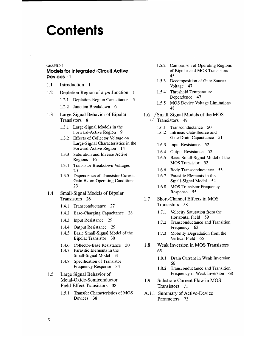
Contents
CHAPTER 1
Models for Integrated-Circuit Active
Devices 1
1.1
1.2 Depletion Region of a pn Junction 1
1.2.1 Depletion-Region Capacitance 5
1.2.2 JunctionBreakdown 6
Introduction 1
1.3 Large-Signal Behavior of Bipolar
Transistors 8
1.3.1 Large-Signal Models in the
Forward-Active Region 9
1.3.2 Effects of Collector Voltage on
Large-Signal Characteristics in the
Forward-Active Region 14
1.3.3 Saturation and Inverse Active
Regions 16
1.3.4 Transistor Breakdown Voltages
20
1.3.5 Dependence of Transistor Current
Gain PF on Operating Conditions
23
1.4 Small-Signal Models of Bipolar
Transistors 26
1.4.1 Transconductance 27
1.4.2 Base-Charging Capacitance 28
1.4.3 Input Resistance 29
1.4.4 Output Resistance 29
1.4.5 Basic Small-Signal Model of the
Bipolar Transistor 30
1.4.6 Collector-Base Resistance 30
1.4.7 Parasitic Elements in the
Small-Signal Model 3 1
1.4.8 Specification of Transistor
Frequency Response 34
1.5 Large Signal Behavior of
Metal-Oxide-Semiconductor
Field-Effect Transistors 38
1.5.1 Transfer Characteristics of MOS
Devices 38
1 .5.2 Comparison of Operating Regions
of Bipolar and MOS Transistors
45
1 .5.3 Decomposition of Gate-Source
Voltage 47
1.5.4 Threshold Temperature
Dependence 47
1.5.5 MOS Device Voltage Limitations
48
1.6 Small-Signal Models of the MOS
\/Transistors
49
1.6.1 Transconductance 50
1.6.2 Intrinsic Gate-Source and
Gate-Drain Capacitance 51
1.6.4 Output Resistance 52
1.6.5 Basic Small-Signal Model of the
MOS Transistor 52
1.6.6 Body Transconductance 53
1.6.7 Parasitic Elements in the
Small-Signal Model 54
1.6.8 MOS Transistor Frequency
Response 55
1.7 Short-Channel Effects in MOS
Transistors 58
1.7.1 Velocity Saturation from the
Horizontal Field 59
1.7.2 Transconductance and Transition
Frequency 63
1.7.3 Mobility Degradation from the
Vertical Field 65
1.8 Weak Inversion in MOS Transistors
65
1.8.1 Drain Current in Weak Inversion
66
1.8.2 Transconductance and Transition
Frequency in Weak Inversion 68
1.9 Substrate Current Flow in MOS
Transistors 7 1
A. 1.1 Summary of Active-Device
Parameters 73
�
CHAPTER 2
Bipolar, MOS, and BiCMOS
Integrated-Circuit Technology 78
2.1
2.2 Basic Processes in Integrated-Circuit
Introduction 78
Fabrication 79
2.2.1 Electrical Resistivity of Silicon
79
2.2.2 Solid-State Diffusion 80
2.2.3 Electrical Properties of Diffused
Layers 82
2.2.4 Photolithography 84
2.2.5 Epitaxial Growth 85
2.2.6 Ion Implantation 87
2.2.7 Local Oxidation 87
2.2.8 Polysilicon Deposition 87
2.3 High-Voltage Bipolar
Integrated-Circuit Fabrication 88
2.4 Advanced Bipolar Integrated-Circuit
Fabrication 92
2.5 Active Devices in Bipolar Analog
Integrated Circuits 95
2.5.1 Integrated-Circuit npn Transistor
2.5.2 Integrated-Circuit pnp Transistors
96
107
I
I
I
2.6
Passive Components in Bipolar
Integrated Circuits 115
2.6.1 Diffused Resistors 115
2.6.2 Epitaxial and Epitaxial Pinch
Resistors 119
2.6.3 Integrated-Circuit Capacitors 120
2.6.4 Zener Diodes 121
2.6.5 Junction Diodes 122
2.7 Modifications to the Basic Bipolar
Process 123
2.7.1 Dielectric Isolation 123
2.7.2 Compatible Processing for
High-Performance Active Devices
124
2.7.3 High-Performance Passive
Components 127
2.8 MOS Integrated-Circuit Fabrication
127
2.9 Active Devices in MOS Integrated
Circuits 131
4
Contents xi
2.9.1 n-Channel Transistors 13 1
2.9.2 p-Channel Transistors 14 1
2.9.3 Depletion Devices 142
2.9.4 Bipolar Transistors 142
2.10 Passive Components in MOS
Technology 144
2.10.1 Resistors 144
2.10.2 Capacitors in MOS Technology
145
2.10.3 Latchup in CMOS Technology
148
2.11 BiCMOS Technology 150
2.12 Heterojunction Bipolar Transistors
152
Interconnect Delay 153
2.13
2.14 Economics of Integrated-Circuit
Fabrication 154
2.14.1 Yield Considerations in
Integrated-Circuit Fabrication
154
2.14.2 Cost Considerations in
Integrated-Circuit Fabrication
157
2.15 Packaging Considerations for
Integrated Circuits 159
2.15.1 Maximum Power Dissipation 159
2.15.2 Reliability Considerations in
Integrated-Circuit Packaging 162
A.2.1 SPICE Model-Parameter Files 163
CHAPTER 3
Single-Transistor and Multiple-Transistor
Amplifiers 170
3.1 Device Model Selection for
Approximate Analysis of Analog
Circuits 171
3.2 Two-Port Modeling of Amplifiers 172
3.3 Basic Single-Transistor Amplifier
Stages 174
3.3.1 Common-Emitter Configuration
175
3.3.2 Common-Source Configuration
179
3.3.3 Common-Baseconfiguration 183
3.3.4 Common-Gate Configuration 186
�




 2023年江西萍乡中考道德与法治真题及答案.doc
 2012年重庆南川中考生物真题及答案.doc
 2013年江西师范大学地理学综合及文艺理论基础考研真题.doc
 2020年四川甘孜小升初语文真题及答案I卷.doc
 2020年注册岩土工程师专业基础考试真题及答案.doc
 2023-2024学年福建省厦门市九年级上学期数学月考试题及答案.doc
 2021-2022学年辽宁省沈阳市大东区九年级上学期语文期末试题及答案.doc
 2022-2023学年北京东城区初三第一学期物理期末试卷及答案.doc
 2018上半年江西教师资格初中地理学科知识与教学能力真题及答案.doc
 2012年河北国家公务员申论考试真题及答案-省级.doc
 2020-2021学年江苏省扬州市江都区邵樊片九年级上学期数学第一次质量检测试题及答案.doc
 2022下半年黑龙江教师资格证中学综合素质真题及答案.doc