logo资料库

PN532介绍.里面有详细列子.pdf

第1页 / 共70页
第2页 / 共70页
第3页 / 共70页
第4页 / 共70页
第5页 / 共70页
第6页 / 共70页
第7页 / 共70页
第8页 / 共70页
资料共70页,剩余部分请下载后查看
Introduction
Interfaces with the host controller
PN532 block diagram
PN532 host link protocol
Standard frame
Extended frame
Additional lines (IRQ only or IRQ and H_REQ)
Typical application diagram
Default pin configuration
How to interface with the PN532?
SPI interface
Sequence to use communicate in SPI
SPI mode selection
I2C interface
Handshake mode in I2C
The PN532 is not in power down, the host controller initiate
The PN532 may be in power down, the host controller initiate
The PN532 is in power down, after TgInitAsTarget command.
Virtual card mode.
Recommended operating conditions
HSU interface
Baudrate
How to change HSU speed in SCRTester?
Handshake mode in HSU
The PN532 is not in power down, the host controller initiate
The PN532 may be in power down, the host controller initiate
The PN532 is in power down, after TgInitAsTarget command.
Virtual card mode.
The PN532 commands
Global view
The PN532 embedded software API: commands and errors lists
Commands codes
Errors codes
The PN532 various modes
RFConfiguration command
How to use the PN532 as a Mifare reader?
Timeout and number of retries
Activation phase (InListPassiveTarget command)
Communication phase (InDataExchange command)
Deactivation phase (InDeselect/InRelease command)
How to use the PN532 as a T=CL reader (ISO/IEC 14443-4)?
Timeout and number of retries
Activation phase (InListPassiveTarget command)
Communication phase (InDataExchange command)
Deactivation phase (InDeselect/InRelease command)
How to use the PN532 as a DESfire cards reader?
Timeout and number of retries
How to use the PN532 as a FeliCa reader?
Timeout and number of retries
Activation phase (InListPassiveTarget command)
Communication phase (InDataExchange command)
Deactivation phase (InDeselect/InRelease command)
How to use the PN532 as a Jewel cards reader ?
How to use the PN532 as a reader for several types of cards
How to use the PN532 in a NFC peer-to-peer communication?
How to use the PN532 as an initiator in a NFC peer-to-peer c
About PSL (Parameter Selection)
About InDeselect command
Timeout and number of retries
How to use the PN532 as a target in a NFC peer-to-peer commu
What are default timeout values of the PN532 as a target?
How to fill TgInitAsTarget parameters?
Handling of several cards/targets
Transfer of large amount of data
Chaining mechanism
Metachaining mechanism
Effective throughput
How to emulate a ISO/IEC 1443-4A card ?
How to use Smart connectivity (combination of the PN532 and
Virtual card mode
Wired card mode
Dual card mode
Application schematics
Recommendations
Recommendations/ known limitations
Legal information
Definitions
Disclaimers
Licenses
Patents
Trademarks
Contents
AN<10449_1> PN532 application note Rev. <01.00> — 07 December 2006 Application note Document information Info Content Keywords Abstract NFC, ISO/IEC 18092, the PN532A3HN/C104 The PN532 Application note. How to use the PN532 as a reader, as a card, or in a NFC peer-to-peer communication.
NXP Semiconductors Revision history Rev Date 1.0 <0.1> 2006 Dec 14 <2006-09-25> Description First release creation AN<10449 1> PN532 application note Contact information For additional information, please visit: http://www.nxp.com For sales office addresses, please send an email to: sales.addresses@www.nxp.com Application note Rev. <01.00> — 07 December 2006 © NXP B.V. 2006. All rights reserved. 2 of 70
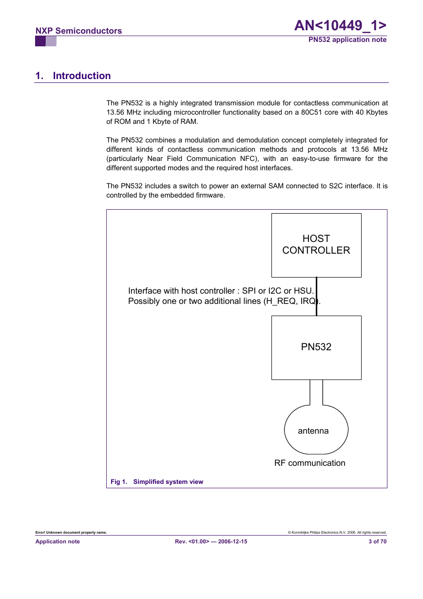
NXP Semiconductors AN<10449_1> PN532 application note 1. Introduction The PN532 is a highly integrated transmission module for contactless communication at 13.56 MHz including microcontroller functionality based on a 80C51 core with 40 Kbytes of ROM and 1 Kbyte of RAM. The PN532 combines a modulation and demodulation concept completely integrated for different kinds of contactless communication methods and protocols at 13.56 MHz (particularly Near Field Communication NFC), with an easy-to-use firmware for the different supported modes and the required host interfaces. The PN532 includes a switch to power an external SAM connected to S2C interface. It is controlled by the embedded firmware. HOST CONTROLLER Interface with host controller : SPI or I2C or HSU. Possibly one or two additional lines (H_REQ, IRQ). PN532 antenna RF communication Fig 1. Simplified system view Error! Unknown document property name. Application note Rev. <01.00> — 2006-12-15 © Koninklijke Philips Electronics N.V. 2006. All rights reserved. 3 of 70
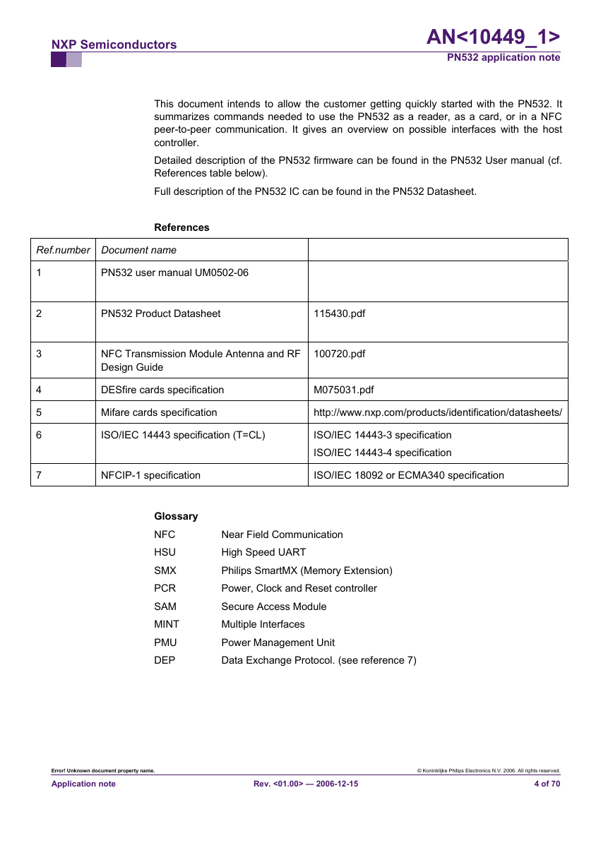
Ref.number Document name PN532 user manual UM0502-06 PN532 Product Datasheet 1 2 3 4 5 6 7 NXP Semiconductors AN<10449_1> PN532 application note This document intends to allow the customer getting quickly started with the PN532. It summarizes commands needed to use the PN532 as a reader, as a card, or in a NFC peer-to-peer communication. It gives an overview on possible interfaces with the host controller. Detailed description of the PN532 firmware can be found in the PN532 User manual (cf. References table below). Full description of the PN532 IC can be found in the PN532 Datasheet. References 115430.pdf NFC Transmission Module Antenna and RF Design Guide 100720.pdf DESfire cards specification M075031.pdf Mifare cards specification http://www.nxp.com/products/identification/datasheets/ ISO/IEC 14443 specification (T=CL) ISO/IEC 14443-3 specification ISO/IEC 14443-4 specification NFCIP-1 specification ISO/IEC 18092 or ECMA340 specification Glossary NFC HSU SMX PCR SAM MINT PMU DEP Near Field Communication High Speed UART Philips SmartMX (Memory Extension) Power, Clock and Reset controller Secure Access Module Multiple Interfaces Power Management Unit Data Exchange Protocol. (see reference 7) Error! Unknown document property name. Application note Rev. <01.00> — 2006-12-15 © Koninklijke Philips Electronics N.V. 2006. All rights reserved. 4 of 70
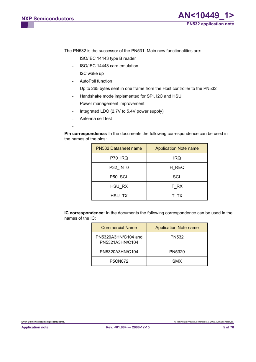
NXP Semiconductors AN<10449_1> PN532 application note The PN532 is the successor of the PN531. Main new functionalities are: ISO/IEC 14443 type B reader ISO/IEC 14443 card emulation I2C wake up - - - - AutoPoll function - Up to 265 bytes sent in one frame from the Host controller to the PN532 - Handshake mode implemented for SPI, I2C and HSU - Power management improvement - - Antenna self test - Integrated LDO (2.7V to 5.4V power supply) Pin correspondence: In the documents the following correspondence can be used in the names of the pins: PN532 Datasheet name Application Note name P70_IRQ P32_INT0 P50_SCL HSU_RX HSU_TX IRQ H_REQ SCL T_RX T_TX IC correspondence: In the documents the following correspondence can be used in the names of the IC: Commercial Name Application Note name PN5320A3HN/C104 and PN5321A3HN/C104 PN5320A3HN/C104 P5CN072 PN532 PN5320 SMX Error! Unknown document property name. Application note Rev. <01.00> — 2006-12-15 © Koninklijke Philips Electronics N.V. 2006. All rights reserved. 5 of 70
NXP Semiconductors AN<10449_1> PN532 application note 2. Interfaces with the host controller 2.1 PN532 block diagram The PN532 is based on an 8051 core, with 40 Kbytes of ROM and 1Kbyte of RAM. The chip contains a contactless UART, a contactless front end, a “PCR” block that controls clocks and power. It can be connected to the host controller in I2C, SPI or HSU (High Speed UART). One or two more lines (IRQ and H_REQ) can be added. The interface is selectable using I0 and I1 pins. A SAM companion chip can be attached using S2C interface. A part of the IC can be powered directly from a mobile battery (VBAT between 2.7V and 5.4V). The Pad power supply (PVDD) must be between 1.6V and 3.6V. The SAM power supply SVDD is provided by the PN532. P30 P31 P32 P33 IRQ I0 I1 RS232 I2C 8051 ROM 40 kbyte RAM 1 kbyte SCK or P72 MISO or P71 MOSI or SDA or D- or Tx NSS or SCL or D+ or Rx MINT HSU FIFO SPI ContactLess UART FIFO, Mifare Classic Unit, Frame generation and check Power switch, regulator, LDO, power on reset RSTPD SVDD (output) power for SAM interface VDD (1.6 V to 3.6V) PCR (Power Clock and Reset controller) ContactLess Front End RF Detector, Demod, Antenna driver SIGIN SIGOUT P34 RX LOADMOD VBAT (2.7 to 5.4V) OSC 27.12MHz Xtal TX1 TX2 Fig 2. PN532 block diagram Error! Unknown document property name. Application note Rev. <01.00> — 2006-12-15 © Koninklijke Philips Electronics N.V. 2006. All rights reserved. 6 of 70
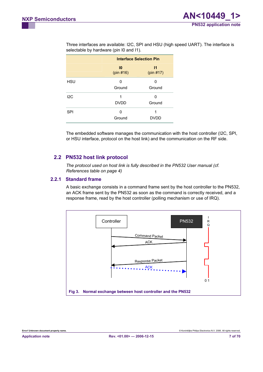
NXP Semiconductors AN<10449_1> PN532 application note Three interfaces are available: I2C, SPI and HSU (high speed UART). The interface is selectable by hardware (pin I0 and I1). HSU I2C SPI Interface Selection Pin I0 (pin #16) 0 Ground 1 DVDD 0 Ground I1 (pin #17) 0 Ground 0 Ground 1 DVDD The embedded software manages the communication with the host controller (I2C, SPI, or HSU interface, protocol on the host link) and the communication on the RF side. 2.2 PN532 host link protocol The protocol used on host link is fully described in the PN532 User manual (cf. References table on page 4) 2.2.1 Standard frame A basic exchange consists in a command frame sent by the host controller to the PN532, an ACK frame sent by the PN532 as soon as the command is correctly received, and a response frame, read by the host controller (polling mechanism or use of IRQ). Controller PN532 I R Q Command Packet ACK Response Packet ACK Fig 3. Normal exchange between host controller and the PN532 0 1 Error! Unknown document property name. Application note Rev. <01.00> — 2006-12-15 © Koninklijke Philips Electronics N.V. 2006. All rights reserved. 7 of 70
NXP Semiconductors AN<10449_1> PN532 application note Command and response frame structure is shown in figure 3. 00 00 FF LEN LCS TFI PD0 PD1 ……... PDn DCS 00 Fig 4. Information frame Postamble Packet Data Checksum Packet Data Specific PN532 Frame Identifier Packet Length Checksum Packet Length Start of Packet Code Preamble PREAMBLE 1 byte START CODE 2 bytes (00h and FFh) LEN LCS TFI (TFI and PD0 to PDn) 1 byte indicating the number of bytes in the data field 1 Packet Length Checksum LCS byte that satisfies the relation: 1 byte the PN532 Frame Identifier, the value of this byte depends on the way of the message Lower byte of [LEN + LCS] = 00h - D4h in case of a frame from the system controller to the the PN532 - D5h in case of a frame from the the PN532 to the system controller DATA 1 Data Checksum DCS byte that satisfies the relation: LEN-1 bytes of Packet Data Information The first byte PD0 is the Command Code DCS Lower byte of [TFI + PD0 + PD1 + … + PDn + DCS] = 00h POSTAMBLE 1 byte ACK frame is described in figure 4. 00 00 FF 00 FF 00 Postamble ACK Packet Code Start of Packet Code Preamble Fig 5. ACK frame List of available commands (PD0 byte) is provided in paragraph 3.2 on page 25. Error! Unknown document property name. Application note Rev. <01.00> — 2006-12-15 © Koninklijke Philips Electronics N.V. 2006. All rights reserved. 8 of 70
分享到:
收藏