W86L388
Programming Information
�
6. REGISTER
The register in the W86L388 is direct access registers and indirect access registers. The direct access
registers and indirect access registers are listed as follows:
Addr
A[3:1]
Register Name
(note 1)
Direct Access Registers:
000
Command Pipe Reg.
B
15
B
14
B
13
B
12
B
11
B
10
Content (note 2)
B
B
9
6
B
8
B
7
B
5
B
4
Command pipe registers / Response registers
0
0
0
0
-
-
-
-
0
0
Receive data buffer
0
0
Transmit data buffer
0
0
Control
0
0
0
0
0
0
B
3
0
-
B
2
0
-
0
0
B
1
0
-
1
0
B
0
0
-
0
0
X X X X X X X X X X X X X X X X
-
-
-
-
-
-
-
-
(WO)
Response Reg. (RO)
Status Reg. (RO)
Control Reg. (R/W)
Receive Data Buffer
(R/O)
Transmit Data Buffer
(WO)
Interrupt Status Reg.
(RC)
Interrupt Enable Reg.
(R/W)
General I/O Port Data
Reg. (R/W)
General I/O Port
Control Reg. (R/W)
General IP Interrupt
Status Reg. (RC)
General IP Interrupt
Enable Reg. (R/W)
Index Address Reg.
(R/W)
Index Data Register
001
001
010
010
011
011
100
100
101
101
110
111
0
0
-
0
0
0
-
0
0
0
-
0
0
0
0
Status
0
1
-
-
0
0
0
-
0
0
-
0
-
Interrupt status
0
0
-
-
0
-
0
-
0
0
-
0
-
0
0
-
0
-
0
-
0
-
-
0
-
0
-
-
0
-
0
-
-
GIO data
X X X X X
-
-
-
-
-
GIO interrupt status
0
-
0
-
0
-
0
-
-
-
-
-
0
-
-
0
-
0
-
0
-
0
0
-
0
-
0
Interrupt enable
1
0
-
-
0
-
0
-
1
-
0
-
0
-
GIO control
0
0
-
-
0
-
0
-
0
-
GIO interrupt enable
0
0
0
0
0
0
0
Index address
0
0
0
0
0
0
Index data register
0
Indirect Access Registers:
000
Extend Status Reg.
(RO)
000
001
010
011
Setting Reg. (R/W)
Data Format Register
(R/W)
Nac Time-out Register
(R/W)
Error Status Reg. (RO)
X X X X X X X X X X X X X X X X
0
-
W
0
0
0
-
-
0
1
0
-
-
0
1
Extend status
0
-
-
0
0
1
1
Status
0
-
0
1
0
-
0
-
-
0
-
-
-
-
-
Setting register
1
0
0
0
0
Nac time out register
0
1
0
1
Data length
0
1
-
0
1
-
0
1
-
0
1
-
0
1
-
0
1
-
-
0
0
1
-
-
1
0
1
-
�
100
0
0
Test
0
0
Note 1: R/W means the register can be read and write.
Ready & Data Size
Register (R/W)
0
0
0
0
0
0
RO means the register is read only.
RC means the register is read only and read clear.
WO means the register is write only.
0
0
0
0
0
0
F
0
-
0
-
0
-
0
-
0
-
0
-
0
8-
0
Note 2: The data bit in the content is the initial value during hardware reset.
0: the bit value is 0.
1: the bit value is 1.
X: the bit value is unknow.
-: Undefined bit in the register and the value will read 0.
�
6.1 Register Description
6.1.1 Direct Access Registers
Command Pipe Register A[3:1] = 000, Write only:
Bit 15 Bit 14 Bit 13 Bit 12 Bit 11 Bit 10 Bit 9 Bit 8 Bit 7 Bit 6 Bit 5 Bit 4 Bit 3 Bit 2 Bit 1 Bit 0
Command pipe registers
1
Bit 47 Bit 46 Bit 45 Bit 44 Bit 43 Bit 42 Bit 41 Bit 40 Bit 39 Bit 38 Bit 37 Bit 36 Bit 35 Bit 34 Bit 33 Bit 32
Bit 31 Bit 30 Bit 29 Bit 28 Bit 27 Bit 26 Bit 25 Bit 24 Bit 23 Bit 22 Bit 21 Bit 20 Bit 19 Bit 18 Bit 17 Bit 16
Bit 15 Bit 14 Bit 13 Bit 12 Bit 11 Bit10 Bit 9 Bit 8 Bit 7 Bit 6 Bit 5 Bit 4 Bit 3 Bit 2 Bit 1
The 48-bit of SD command is located at the 3 words of command pipe, the Host must write three
words continuously, the first write word is bit 47 to bit 32 of the command, the second write word is
bit 31 to bit 16, the third word is bit 15 to bit 1, bit 0 of the command is 1 always. The 7-bit CRC
code is located at bit [7:1] of command, these bits are ignored and the CRC code will generated
automatically if the CMD_CRC bit in the setting register is enabled. The command will not started
until the three word of the register has been written. When the CMD12 write to the command pipe
register, the time period from the first word write action to the end of third word write action must
longer than the clock period of the system clock.
These registers will be cleared during hardware or software reset.
When the CPU data size is 8-bit, the 48-bit of SD command is located at the 6 bytes of command
pipe, the Host must write six bytes continuously. If the 7-bit CRC code is generated automatically,
the last byte also must write but the content of this byte is ignored.
Response Register A[3:1] = 000, Read only:
Bit 15 Bit 14 Bit 13 Bit 12 Bit 11 Bit 10 Bit 9 Bit 8 Bit 7 Bit 6 Bit 5 Bit 4 Bit 3 Bit 2 Bit 1 Bit 0
48-bit respnse registers
Bit 47 Bit 46 Bit 45 Bit 44 Bit 43 Bit 42 Bit 41 Bit 40 Bit 39 Bit 38 Bit 37 Bit 36 Bit 35 Bit 34 Bit 33 Bit 32
Bit 31 Bit 30 Bit 29 Bit 28 Bit 27 Bit 26 Bit 25 Bit 24 Bit 23 Bit 22 Bit 21 Bit 20 Bit 19 Bit 18 Bit 17 Bit 16
Bit 15 Bit 14 Bit 13 Bit 12 Bit 11 Bit10 Bit 9 Bit 8 Bit 7 Bit 6 Bit 5 Bit 4 Bit 3 Bit 2 Bit 1
Bit 15 Bit 14 Bit 13 Bit 12 Bit 11 Bit 10 Bit 9 Bit 8 Bit 7 Bit 6 Bit 5 Bit 4 Bit 3 Bit 2 Bit 1 Bit 0
1
0
0
0
0
0
0
Bit
130
Bit
114
Bit
Bit
128
131
Bit
Bit
115
112
Bit 99 Bit 98 Bit 97 Bit 96
Bit
129
Bit
113
0
136-bit respnse registers
0
Bit
134
Bit
118
Bit
102
Bit
135
Bit
119
Bit
103
Bit
120
Bit
104
Bit
121
Bit
105
Bit
133
Bit
117
Bit
101
Bit
132
Bit
116
Bit
100
Bit
122
Bit
106
Bit
123
Bit
107
Bit
124
Bit
108
Bit
126
Bit
110
Bit
125
Bit
109
Bit
127
Bit
111
Bit 95 Bit 94 Bit 93 Bit 92 Bit 91 Bit 90 Bit 89 Bit 88 Bit 87 Bit 86 Bit 85 Bit 84 Bit 83 Bit 82 Bit 81 Bit 80
Bit 79 Bit 78 Bit 77 Bit 76 Bit 75 Bit 74 Bit 73 Bit 72 Bit 71 Bit 70 Bit 69 Bit 68 Bit 67 Bit 66 Bit 65 Bit 64
Bit 63 Bit 62 Bit 61 Bit 60 Bit 59 Bit58 Bit 57 Bit 56 Bit 55 Bit 54 Bit 53 Bit 52 Bit 51 Bit 50 Bit 49 Bit 48
Bit 47 Bit 46 Bit 45 Bit 44 Bit 43 Bit 42 Bit 41 Bit 40 Bit 39 Bit 38 Bit 37 Bit 36 Bit 35 Bit 34 Bit 33 Bit 32
Bit 31 Bit 30 Bit 29 Bit 28 Bit 27 Bit 26 Bit 25 Bit 24 Bit 23 Bit 22 Bit 21 Bit 20 Bit 19 Bit 18 Bit 17 Bit 16
Bit 15 Bit 14 Bit 13 Bit 12 Bit 11 Bit10 Bit 9 Bit 8 Bit 7 Bit 6 Bit 5 Bit 4 Bit 3 Bit 2 Bit 1
The 48-bit or 136-bit card response data may be read this register repeatedly, the first word is bit 47
to 32 of the response if the response is 48 bits, the first word is bit 135 to bit 128 at the data pin of bit
7 to 0 if the response if 136 bits.
These registers will be cleared during hardware or software reset.
1
�
Status Register A[3:1] = 001, Read only:
Bit 15 Bit 14 Bit 13 Bit 12 Bit 11 Bit 10 Bit 9 Bit 8 Bit 7 Bit 6 Bit 5 Bit 4 Bit 3 Bit 2 Bit 1 Bit 0
INT DRQ R2 CMD_
-
RSP
0
DAT_
RV
0
DAT_
TX
0
Buf_
Full
0
Buf_
Epty
1
0
0
0
-
-
-
-
-
-
-
INT (Interrupt): This bit = 1 when the interrupt input becomes active (low) regardless any state of
INT_E bit of the interrupt enable register.
DRQ (DMA request): This bit = 1 when DMA request input (DRQN) becomes active (low).
R2 (R2 response): This bit reflects the data stored in the response registers are the R2 response and
136 bits effective. The 48-bit of response is stored if this bit = 0. This bit will updated if the card
response has been received and RSP bit (bit 12) of this register is active.
CMD_RSP (Card command response): This bit indicates that the response from the card has been
received and R2 status is updated. This bit will be cleared automatically if the Host read response
data.
Buf_Epty (Buffer empty): This bit = 1 when the command is receive data on the data line and the
receive data buffer is empty or when the command is transmit data on the data line and the transmit
data buffer is empty. The receive and transmit data buffer will set to empty during reset.
Buf_Full (Buffer full): This bit = 1 when the command is receive data on the data line and the receive
data buffer is full or when the command is transmit data on the data line and the transmit data buffer
is full.
DAT_TX (Data transmit): This bit indicates the data will transmit to the card on the data line. It will
reset to low when the command has been executed completedly.
DAT_RV (Data receive): This bit indicates the data receive from the card on the data line. It will set
high when the command pipe of read command has been write completedly and will reset to low
when the data length and CRC-16 has been received and the receive data buffer has been read out
completedly. In multi block read operation, this bit stays in high until the STOP_TRANSMISSION
command is written. The buffer status bits of Buf_Epty and Buf_Full reflect the status of receive data
buffer if this bit is high, the Buf_Epty and Buf_Full reflect the status of transmit data buffer if this bit
is low.
Bit [15:8] of this register will set to default value during hardware or software reset.
Control Register A[3:1] = 001, Read/Write:
Bit 15 Bit 14 Bit 13 Bit 12 Bit 11 Bit 10 Bit 9 Bit 8 Bit 7 Bit 6 Bit 5
PWD RST DBF_
RST
0
Bit 4 Bit 3 Bit 2 Bit 1 Bit 0
SIEN
PWD (Power down): This bit = 1 is used to power down the internal logic and crystal driver. Set this
bit to low will enabled the W86L388 when the W86L388 is in power down state. But the W86L388
will never enabled if Host interface type 2 is configured and the Host I/F clock (HCKI) input is
disabled.
RST (Reset): This bit = 1 is software reset and is used to reset the internal logic and receive and
transmit data buffer, the content of other registers are not affected. The command register pipe and
response registers will be cleared. This bit will return to low after software reset.
DBF_RST (Data buffer reset): This bit is used to reset the receive and transmit data buffer, it will
return to low automatically after the data buffer have been reset.
C_CLKS
0
0
0
0
1
0
0
-
-
-
-
-
-
-
-
�
SIEN (Serial interface enable): The SD/MMC bus interface is enabled when this bit is high. It may be
disabled if card is not exist or during the card is programming. The CLK of SD/MMC may be
disabled by writing this bit to low during the card is programming.
C_CLKS (System and card clock set): These bits are used to set the clock frequency of the system
and card, 0010 = XTI clock/8192, 0011 = XTI clock/4096, 0100 = XTI clock/2048, 0101 = XTI
clock/1024, 0110 = XTI clock/512, 0111 = XTI clock/256, 1000 = XTI clock/128, 1001 = XTI
clock/64, 1010 = XTI clock/32, 1011 = XTI clock/16, 1100 = XTI clock/8, 1101 = XTI clock/4, 1110
= XTI clock/2, 1111 = XTI clock.
Bit 7 and Bit [5:0] of this register will remained unchange during software reset.
Receive Data Buffer Register A[3:1] = 010, Read only:
Bit 15 Bit 14 Bit 13 Bit 12 Bit 11 Bit 10 Bit 9 Bit 8 Bit 7 Bit 6 Bit 5 Bit 4 Bit 3 Bit 2 Bit 1 Bit 0
Receive data buffer
0
0
0
0
0
0
0
0
0
0
0
0
0
0
0
0
Receive Data Buffer Register A[3:0] = 0100, Read only, 8-bit data size:
Bit 7 Bit 6 Bit 5 Bit 4 Bit 3 Bit 2 Bit 1 Bit 0
Receive data buffer
0
0
0
0
0
0
0
0
The data received from the DAT pin or DAT[3:0] pins will be recorded in receive data buffer if the
data read on the data line, the BUF_Epty and BUF_Full bits in the status register will reflect the
buffer status and XDRQN will actived. The received data can be read out by reading this register
repeatedly until receive data buffer is empty. Only high byte data (bit [15:8]) is valid if the last data is
one byte only.
The data is located at bit[7:0] and address bit 0 must set 0 when read the receive data buffer register
with 8-bit data size is configured.
Transmit Data Buffer Register A[3:1] = 010, Write only:
Bit 15 Bit 14 Bit 13 Bit 12 Bit 11 Bit 10 Bit 9 Bit 8 Bit 7 Bit 6 Bit 5 Bit 4 Bit 3 Bit 2 Bit 1 Bit 0
Transmit data buffer
X
X
X
X
X
X
X
X
X
X
X
Transmit Data Buffer Register A[3:0] = 0100, Write only, 8-bit data size:
X
X
X
X
X
Bit 7 Bit 6 Bit 5 Bit 4 Bit 3 Bit 2 Bit 1 Bit 0
Transmit data buffer
X
X
X
X
X
X
X
X
The data stored in the transmit data buffer will transmitted to the DAT pin or DAT[3:0] pins if the
data will write to the card on the data line, the BUF_Epty and BUF_Full bits in the status register will
reflect the buffer status and XDRQN will actived. The transmit data must be writen to this register
repeatedly until the data size specified in the command register is enough. Only high byte data
(bit[15:8]) is valid if the last data is one byte only.
The data is located at bit [7:0] and address bit 0 must set 0 when write the transmit data buffer
register with 8-bit data size of Host CPU.
Interrupt Status Register A[3:1] = 011, Read only and Read Clear:
�
Bit 8 Bit 7 Bit 6 Bit 5 Bit 4 Bit 3 Bit 2 Bit 1 Bit 0
-
TOE
-
-
-
-
-
-
-
Bit 15 Bit 14 Bit 13 Bit 12 Bit 11 Bit 10 Bit 9
CRC7 CRC16/
CMDE PRGE DREQ GIT
Cwr_
ERR
INS/
Cwr_
RSP
0
0
0
0
0
0
0
0
CMDE (Command ended): Command ended and response received if the command response is
needed. This bit will be cleared if the Host start write command pipe register.
PRGE (Program ended): Program ended or next block of data can be transmitted in block write
command or multi block write command. This bit will active at the end of the busy state on the DAT
signal. This bit will be cleared if the Host start write command pipe register.
DREQ (DMA request interrupt in): This bit = 1 when the data transfer is requested.
GIT (General IO interrupt in): This bit = 1 when the enabled general input port goes low.
INS/Cwr_RSP: The INS interrupt in is effective when SIEN bit in the control register is low, the
Cwr_RSP interrupt in is effective when SIEN bit is high.
INS (Card insert/remove interrupt in): This bit = 1 if CD/DAT3 pin goes high or goes low. This bit
indicates the card is inserting or removing and the XINTN will be actived even if the chip is in power
down state and when INS_IE and INT_E in the interrupt enable register is configured in high. This bit
will not affected when the SD data bit is 4-bit width and the data will transfer on the data line.
Cwr_RSP (Card write data response): This bit indicates that the CRC status or programming status of
the write data has been received, if write data CRC error occurs or programming error occurs the
error status will reflected on the CRC16/Cwr_ERR.
CRC7 (Response CRC error interrupt): This bit = 1 when the received response with CRC error
checked. This bit will be disabled when NO_CRC bit is set in the control register.
CRC16/Cwr_ERR (Data CRC error or Card write error interrupt): This bit = 1 when the received data
with CRC error checked if read data from the card, it will be disabled when NO_CRC bit is set in the
control register. This bit will set high if the write data CRC error occurs or programming error occurs
from the card and regardless the state of NO_CRC bit. The Host should read Cpg_ERR bit of the
error status register to check is CRC error or programming error.
TOE (Time out error interrupt): This bit = 1 when any one of the time out error occurs.
The XINTN goes low when any bit of interrupt status register becomes high, the XINTN signal will
return to high and the interrupt status register will cleared when read the interrupt status register. The
related bit in the interrupt status register also will be recorded but INT bit in the status register and
XINTN pin will not activated if the related interrupt enable bit is disabled.
Bit [15:8] of this register will be cleared during hardware or software reset.
Interrupt Enable Register A[3:1] = 011, Read/Write:
Bit 15 Bit 14 Bit 13 Bit 12 Bit 11 Bit 10 Bit 9 Bit 8
-
Bit 7
CMDE_
Bit 5
DREQ_
Bit 6
PRGE_
-
-
-
-
-
-
-
Bit 4 Bit 3 Bit 2 Bit 1 Bit 0
GIT_
INT_
IE
E
CRC_
IE
TOE_
IE
IE
IE
IE
INS_
IE/
Cwr_
RSP_
IE
0
0
0
0
0
1
1
0
The interrupt status will reflect the status and the XINTN pin will active if the related bit interrupt is
enabled and global interrupt enable bit is enabled. The interrupt status bit will be recorded but INT bit
in the status register and XINTN pin will not active if the related bit of this register is disabled.
CMDE_IE (Command ended interrupt enable):
PRGE_IE (Program ended interrupt enable):
�
DREQ_IE (DMA request interrupt enable):
GIT_IE (General IO interrupt enable):
INS_IE/Cwr_RSP_IE (Card insert or Card write Response interrupt enable): The INS_IE can be
programmed or read when SIEN bit in the control register is low and Cwr_RSP_IE can be
programmed or read when SIEN bit is high.
CRC_IE (CRC7 and CRC16/Cwr_ERR interrupt enable): This bit is used to enable both CRC7 and
CRC16/Cwr_ERR interrupt.
TOE_IE (Time out interrupt enable):
INT_E (Global interrupt enable): The interrupt pin XINTN will not actived if this bit is disabled, the
interrupt status register and INT bit in the status register are not affected.
Bit [7:0] of this register will remained unchange during software reset.
General I/O Port Data Register A[3:1] = 100, Read/Write:
Bit 15 Bit 14 Bit 13 Bit 12 Bit 11 Bit 10 Bit 9 Bit 8 Bit 7 Bit 6 Bit 5 Bit 4 Bit 3 Bit 2 Bit 1 Bit 0
-
-
-
-
-
-
-
-
-
-
- GIN4/
GO4
X
0
GIN3/
GO3
X
GIN2/
GO2
X
GIN1/
GO1
X
GIN0/
GO0
X
0
0
GIN[4:0]: is the read data from general input port [4:0] pins. The read bit is high when the input pin
is low.
GO[4:0]: is the data output to the GO[4:0] pins, write 1 in the register will output high on the related
GO pin. The read value will be the same as write value when the GIO[4:0] is defined as output.
General I/O Port Control Register A[3:1] = 100, Read/Write:
Bit 15 Bit 14 Bit 13 Bit 12 Bit 11 Bit 10 Bit 9 Bit 8 Bit 7 Bit 6 Bit 5 Bit 4 Bit 3 Bit 2 Bit 1 Bit 0
GOEN
- GOEN
GOEN
GOEN
GOEN
-
-
-
-
-
-
-
-
-
-
0
0
0
4
0
3
0
2
0
1
0
0
0
GOEN[4:0] (General output enable): The bit = 1 is used to enable the related general output pin of
GO[4:0].
Bit [4:0] of this register will remained unchange during software reset.
General IO Port Interrupt Status Register A[3:1] = 101, Read Only and Read Clear:
Bit 15 Bit 14 Bit 13 Bit 12 Bit 11 Bit 10 Bit 9 Bit 8 Bit 7 Bit 6 Bit 5 Bit 4 Bit 3 Bit 2 Bit 1 Bit 0
-
-
-
-
-
-
-
-
-
0
-
0
-
0
GIT4 GIT3 GIT2 GIT1 GIT0
0
0
0
0
0
GIT0 (General input output interrupt): The bit = 1 indicates the GIO0 pin has been change state (goes
from high to low or from low to high), read this register will clear the GIT0 to low.
GIT[4:1] (General input output interrupt): The bit = 1 indicates the related GIO pin has been actived
(low), read this register will clear the general IO port interrupt status to low if the related GIO[4:1] is
high.
Bit [12:8] of this register will be cleared during hardware or software reset.
General IO Port Interrupt Enable Register A[3:1] = 101, Read/Write:
Bit 15 Bit 14 Bit 13 Bit 12 Bit 11 Bit 10 Bit 9 Bit 8 Bit 7 Bit 6 Bit 5 Bit 4 Bit 3 Bit 2 Bit 1 Bit 0
GIT_
EN0
0
GIT_
EN4
0
GIT_
EN3
0
GIT_
EN2
0
GIT_
EN1
0
0
0
0
-
-
-
-
-
-
-
-
-
-
-
�


 Meta大模型论文:The Llama 3 Herd of Models.pdf
 ACS0709(传感器资料).PDF
 495个C语言常见问题集.pdf
 CS型可燃性气体传感器(106型和1003型)(传感器资料).pdf
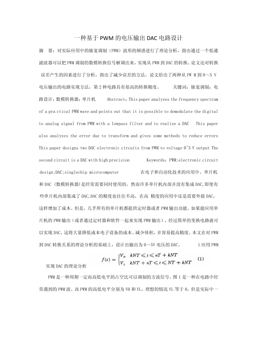 一种基于PWM的电压输出DAC电路设计.pdf
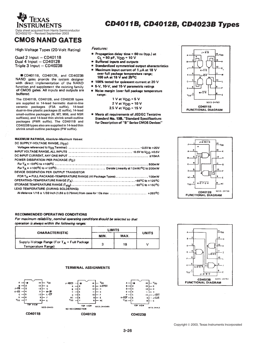 cd4011b(智能车电机驱动).pdf
 电路设计规范_中兴.pdf
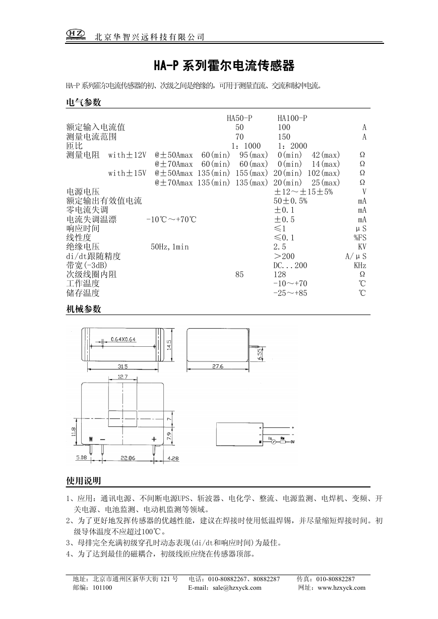 HA50-P(传感器资料).pdf
 ETD-core(TDK磁芯资料).pdf