ACS709
High Bandwidth, Fast Fault Response Current Sensor IC
In Thermally Enhanced Package
Features and Benefits
▪ Industry-leading noise performance with 120 kHz
bandwidth through proprietary amplifier and filter
design techniques
▪ Integrated shield greatly reduces capacitive coupling
from current conductor to die due to high dV/dt, and
prevents offset drift in high-side applications
▪ Small footprint surface mount QSOP24 package
▪ 2100 VRMS isolation voltage between primary current
path and sensor IC electronics
▪ 1.1 mΩ primary conductor resistance for low power loss
▪ User-settable Overcurrent Fault level
▪ Overcurrent Fault signal typically responds to an
overcurrent condition in < 2 μs
▪ Filter pin capacitor sets analog signal bandwidth
▪ ±2% typical output error
▪ 3 to 5.5 V, single supply operation
▪ Factory trimmed sensitivity, quiescent output voltage,
and associated temperature coefficients
▪ Chopper stabilization results in extremely stable
quiescent output voltage
▪ Ratiometric output from supply voltage
Package: 24 pin QSOP (suffix LF)
Approximate Scale
Description
The Allegro® ACS709 current sensor IC provides economical
and precise means for current sensing applications in industrial,
automotive, commercial, and communications systems. The
device is offered in a small footprint surface mount package
that allows easy implementation in customer applications.
The ACS709 consists of a precision linear Hall sensor integrated
circuit with a copper conduction path located near the surface
of the silicon die. Applied current flows through the copper
conduction path, and the analog output voltage from the Hall
sensor IC linearly tracks the magnetic field generated by the
applied current. The accuracy of the ACS709 is maximized
with this patented packaging configuration because the Hall
element is situated in extremely close proximity to the current
to be measured.
High level immunity to current conductor dV/dt and stray
electric fields, offered by Allegro proprietary integrated shield
technology, guarantees low output ripple and low offset drift
in high-side applications.
The voltage on the Overcurrent Input (VOC pin) allows
customers to define an overcurrent fault threshold for the
device. When the current flowing through the copper conduction
path (between the IP+ and IP– pins) exceeds this threshold,
Continued on the next page…
Typical Application
IP
1
2
3
4
5
6
7
8
9
10
11
12
IP+
IP+
IP+
IP+
IP+
IP+
IP–
IP–
IP–
IP–
IP–
IP–
ACS709
NC
NC
FAULT_EN
VOC
VCC
FAULT
VIOUT
FILTER
VZCR
GND
NC
NC
24
23
22
21
20
19
18
17
16
15
14
13
Fault_EN
RH
VCC
RL
330 kΩ
B
0.1 μF
COC
VIOUT
CF
1 nF
A
RH, RL Sets resistor divider reference for VOC
CF
COC
A
B
Noise and bandwidth limiting filter capacitor
Fault delay setting capacitor, 22 nF maximum
Use of capacitor required
Use of resistor optional
ACS709-DS
�
ACS709
High Bandwidth, Fast Fault Response Current Sensor IC
In Thermally Enhanced Package
Description (continued)
the open drain Overcurrent Fault pin will transition to a logic low
state. Factory programming of the linear Hall sensor IC inside of
the ACS709 results in exceptional accuracy in both analog and
digital output signals.
The internal resistance of the copper path used for current sensing is
typically 1.1 mΩ, for low power loss. Also, the current conduction
path is electrically isolated from the low voltage device inputs and
outputs. This allows the ACS709 family of sensor ICs to be used
in applications requiring electrical isolation, without the use of
opto-isolators or other costly isolation techniques.
Applications include:
• Motor control and protection
• Load management and overcurrent detection
• Power conversion and battery monitoring / UPS systems
Selection Guide
Part Number
IP(LIN)
(A)
75
ACS709LLFTR-35BB-T
ACS709LLFTR-20BB-T
37.5
*Contact Allegro for packing options.
Absolute Maximum Ratings
Characteristic
Supply Voltage
Filter Pin
Analog Output Pin
Overcurrent Input Pin
Overcurrent ¯F¯ ¯A ¯U ¯¯L¯ ¯T¯ Pin
Fault Enable (FAULT_EN) Pin
Voltage Reference Output Pin
DC Reverse Voltage: Supply Voltage, Filter, Analog
Output, Overcurrent Input, Overcurrent Fault, Fault
Enable, and Voltage Reference Output Pins
Isolation Voltage
Output Current Source
Output Current Sink
Operating Ambient Temperature
Junction Temperature
Storage Temperature
(Typ at VCC = 5 V)
Sens
(mV/A)
28
56
Symbol
VCC
VFILTER
VIOUT
VOC
V ¯F¯ ¯A ¯U ¯¯L¯ ¯T¯
VFAULTEN
VZCR
VRdcx
VISO
IIOUT(Source)
IIOUT(Sink)
TA
TJ(max)
Tstg
TA
(°C)
Packing*
–40 to 150
Tape and Reel, 2500 pieces per reel
Notes
Rating
Units
8
8
32
8
8
8
8
–0.5
2100
3
1
–40 to 150
165
–65 to 170
V
V
V
V
V
V
V
V
VAC
mA
mA
°C
°C
°C
60 Hz AC, TA = 25°C, 1 minute
Range L
Allegro MicroSystems, Inc.
115 Northeast Cutoff
Worcester, Massachusetts 01615-0036 U.S.A.
1.508.853.5000; www.allegromicro.com
2
�
ACS709
High Bandwidth, Fast Fault Response Current Sensor IC
In Thermally Enhanced Package
Functional Block Diagram
VCC
Hall
Bias
POR
FAULT_EN
VOC
IP+
IP–
Sensitivity
Trim
Signal
Recovery
Hall
Amplifier
Fault
Comparator
–
+
RF(INT)
GND
FILTER
POR
FAULT Reset
–
+
2VREF
Q
D
CLK
R
Drain
FAULT
Control
Logic
3 mA
VZCR
VIOUT
VOUT(Q)
Trim
Description
Terminal List Table
Name
Number
Pin-out Diagram
IP+
IP+
IP+
IP+
IP+
IP+
IP–
IP–
IP–
IP–
IP–
IP–
1
2
3
4
5
6
7
8
9
10
11
12
24
23
22
21
20
19
18
17
16
15
14
13
NC
NC
FAULT_EN
VOC
VCC
FAULT
VIOUT
FILTER
VZCR
GND
NC
NC
1 through 6
7 through 12
13, 14, 23, 24
15
16
17
18
19
20
21
22
Sensed current copper conduction path pins. Terminals for current being sensed;
fused internally, loop to IP– pins; unidirectional or bidirectional current flow.
Sensed current copper conduction path pins. Terminals for current being sensed;
fused internally, loop to IP+ pins; unidirectional or bidirectional current flow.
No connection
Device ground connection.
Voltage Reference Output pin. Zero current (0 A) reference; output voltage on this
pin scales with VCC .
Filter pin. Terminal for an external capacitor connected from this pin to GND to set
the device bandwidth.
Analog Output pin. Output voltage on this pin is proportional to current flowing
through the loop between the IP+ pins and IP– pins.
VIOUT
¯F¯ ¯A ¯U ¯¯L¯ ¯T¯ Overcurrent Fault pin. When current flowing between IP+ pins and IP– pins
VCC
exceeds the overcurrent fault threshold, this pin transitions to a logic low state.
Supply voltage.
Overcurrent Input pin. Analog input voltage on this pin sets the overcurrent fault
threshold.
IP+
IP–
NC
GND
VZCR
FILTER
VOC
FAULT_EN Enables overcurrent faulting when high. Resets ¯F¯ ¯A ¯U ¯¯L¯ ¯T¯ when low.
Allegro MicroSystems, Inc.
115 Northeast Cutoff
Worcester, Massachusetts 01615-0036 U.S.A.
1.508.853.5000; www.allegromicro.com
3
�
ACS709
High Bandwidth, Fast Fault Response Current Sensor IC
In Thermally Enhanced Package
Symbol
Test Conditions
COMMON OPERATING CHARACTERISTICS Valid at TA = –40°C to 150°C, VCC = 5 V, unless otherwise specified
Characteristic
Typ.
ELECTRICAL CHARACTERISTICS
Supply Voltage1
Nominal Supply Voltage
Supply Current
Output Capacitance Load
Output Resistive Load
Magnetic Coupling from Device Conductor
to Hall Element
Internal Filter Resistance2
Primary Conductor Resistance
ANALOG OUTPUT SIGNAL CHARACTERISTICS
Full Range Linearity3
Symmetry4
Bidirectional Quiescent Output
TIMING PERFORMANCE CHARACTERISTICS
VIOUT open, ¯F¯ ¯A ¯U ¯¯L¯ ¯T¯ pin high
VIOUT pin to GND
VIOUT pin to GND
VCC
VCCN
ICC
CLOAD
RLOAD
MCHALL
RF(INT)
RPRIMARY
IP = ±IP0A
IP = ±IP0A
IP = 0 A, TA = 25°C
Current flowing from IP+ to IP– pins
–
5
11
–
–
9.5
1.7
1.1
3
–
–
–
10
ELIN
ESYM
VOUT(QBI)
TA = 25°C
Min.
–
–
–
–
–0.75
99.1
±0.25
100
VCC×0.5
VIOUT Signal Rise Time
VIOUT Signal Propagation Time
tr
tPROP
VIOUT Signal Response Time
tRESPONSE
VIOUT Large Signal Bandwidth5
Power-On Time
OVERCURRENT CHARACTERISTICS
Setting Voltage for Overcurrent Switchpoint6
Signal Noise at Overcurrent
Comparator Input
Overcurrent Fault Switchpoint Error7,8
Overcurrent ¯F¯ ¯A ¯U ¯¯L¯ ¯T¯ Pin Output Voltage
Fault Enable (FAULT_EN Pin) Input Low
Voltage Threshold
Fault Enable (FAULT_EN Pin) Input High
Voltage Threshold
Fault Enable (FAULT_EN Pin) Input
Resistance
f3dB
tPO
VOC
INCOMP
EOC
V ¯F¯ ¯A ¯U ¯¯L¯ ¯T¯
VIL
VIH
RFEI
Continued on the next page…
TA = 25°C, Swing IP from 0 A to IP0A,
no capacitor on FILTER pin, 100 pF from
VIOUT to GND
TA = 25°C, no capacitor on FILTER pin,
100 pF from VIOUT to GND
TA = 25°C, Swing IP from 0 A to IP0A,
no capacitor on FILTER pin, 100 pF from
VIOUT to GND
–3 dB, TA = 25°C, no capacitor on FILTER
pin, 100 pF from VIOUT to GND
Output reaches 90% of steady-state level,
no capacitor on FILTER pin, TA = 25°C
–
–
–
–
–
Switchpoint in VOC safe operating area;
assumes INCOMP = 0 A
1 mA sink current at ¯F¯ ¯A ¯U ¯¯L¯ ¯T¯ pin
VCC×0.25
–
–
–
–
0.8 × VCC
–
3
1
4
120
35
–
±1
±5
–
–
–
1
Max.
Units
5.5
–
14.5
10
–
–
–
–
0.75
100.9
–
–
–
–
–
–
VCC×0.4
–
–
0.4
0.1 × VCC
–
–
V
V
mA
nF
kΩ
G/A
kΩ
mΩ
%
%
V
μs
μs
μs
kHz
μs
V
A
%
V
V
V
MΩ
Allegro MicroSystems, Inc.
115 Northeast Cutoff
Worcester, Massachusetts 01615-0036 U.S.A.
1.508.853.5000; www.allegromicro.com
4
�
ACS709
High Bandwidth, Fast Fault Response Current Sensor IC
In Thermally Enhanced Package
COMMON OPERATING CHARACTERISTICS (continued) Valid at TA = –40°C to 150°C, VCC = 5 V, unless otherwise specified
Characteristic
Max.
OVERCURRENT CHARACTERISTICS (continued)
Test Conditions
Symbol
Min.
Typ.
Switchpoint set at 90% of IPOA,
delay from IP exceeding overcurrent
fault threshold to V ¯F¯ ¯A ¯U ¯¯L¯ ¯T¯ < 0.4 V, without
external COC capacitor
Time from VFAULTEN < VIL to
VFAULT > 0.8 × VCC , RPU = 330 kΩ
Time from VFAULTEN pin < VIL to reset of
fault latch; see Functional Block Diagram
TA = 25°C, VOC pin to GND
tOC
tOCR
tOCH
ROC
–
–
–
2
1.9
500
250
–
–
–
–
–
Units
μs
ns
ns
MΩ
Overcurrent Fault Response Time
Overcurrent Fault Reset Delay
Overcurrent Fault Reset Hold Time
Overcurrent Input Pin Resistance
VOLTAGE REFERENCE CHARACTERISTICS
Voltage Reference Output
VZCR
IZCR
∆VZCR
Voltage Reference Output Load Current
TA = 25 °C
Source current
Sink current
V
mA
μA
Voltage Reference Output Drift
mV
1Devices are trimmed for maximum accuracy at VCC = 5 V. The ratiometry feature of the device allows operation over the full VCC range; however, accuracy
may be slightly degraded for VCC values other than 5 V. Contact the Allegro factory for applications that require maximum accuracy for VCC = 3.3 V.
2RF(INT) forms an RC circuit via the FILTER pin.
3This parameter can drift by as much as 0.25% over the lifetime of this product.
4This parameter can drift by as much as 0.3% over the lifetime of this product.
5Calculated using the formula f3dB = 0.35 / tr .
6See page 8 on how to set overcurrent fault switchpoint.
7Switchpoint can be lower at the expense of switchpoint accuracy.
8This error specification does not include the effect of noise. See the INCOMP specification in order to factor in the additional influence of noise on the
fault switchpoint.
–
–
±10
–
3
50
–
0.5 × VCC
–
–
–
–
Allegro MicroSystems, Inc.
115 Northeast Cutoff
Worcester, Massachusetts 01615-0036 U.S.A.
1.508.853.5000; www.allegromicro.com
5
�
ACS709
High Bandwidth, Fast Fault Response Current Sensor IC
In Thermally Enhanced Package
X20B PERFORMANCE CHARACTERISTICS, TA Range L, valid at TA = – 40°C to 150°C, VCC = 5 V, unless otherwise specified
Test Conditions
Min.
–20
–37.5
Typ.
–
–
Max.
20
37.5
Units
A
A
Characteristic
Symbol
IP(OA)
IP(LIN)
Optimized Accuracy Range
Linear Sensing Range
Performance Characteristics at VCC = 5 V
Noise1
Sens
Sensitivity2,3
Electrical Offset Voltage2
VNOISE(rms) TA = 25°C, Sens = 56 mV/A, Cf = 0, CLOAD = 4.7 nF, RLOAD open
mV
mV/A
mV/A
mV/A
mV
mV
mV
%
%
1Vpk-pk noise (6 sigma noise) is equal to 6 × VNOISE(rms). Lower noise levels than this can be achieved by using Cf for applications requiring narrower
bandwidth. See Characteristic Performance page for graphs of noise versus Cf and bandwidth versus Cf.
2See Characteristic Performance Data graphs for parameter distribution over ambient temperature range.
3This parameter can drift by as much as 1.75% over lifetime of the product.
4This parameter can drift by as much as 2.5% over lifetime of the product.
IP = 12.5 A, TA = 25°C
IP = 12.5 A, TA = 25°C to 150°C
IP = 12.5 A, TA = – 40°C to 25°C
IP = 0 A, TA = 25°C
IP = 0 A, TA = 25°C to 150°C
IP = 0 A, TA = – 40°C to 25°C
Tested at IP =12.5 A , IP applied for 5 ms, TA = 25°C to 150°C
Tested at IP =12.5 A , IP applied for 5 ms, TA = – 40°C to 25°C
–
–
54.5
54.5
–
–25
–40
–
–
1.50
56
–
–
±5
–
–
±2
±3
–
–
58
58.5
–
25
40
–
–
Total Output Error2,4
ETOT
VOE
X35B PERFORMANCE CHARACTERISTICS, TA Range L, valid at TA = – 40°C to 150°C, VCC = 5 V, unless otherwise specified
Test Conditions
Min.
–37.5
–75
Typ.
–
–
Max.
37.5
75
Units
A
A
Characteristic
Symbol
IP(OA)
IP(LIN)
Optimized Accuracy Range
Linear Sensing Range
Performance Characteristics at VCC = 5 V
Noise1
Sens
Sensitivity2,3
Electrical Offset Voltage2
VNOISE(rms) TA = 25°C, Sens = 28 mV/A, Cf = 0, CLOAD = 4.7 nF, RLOAD open
mV
mV/A
mV/A
mV/A
mV
mV
mV
%
%
1Vpk-pk noise (6 sigma noise) is equal to 6 × VNOISE(rms). Lower noise levels than this can be achieved by using Cf for applications requiring narrower
bandwidth. See Characteristic Performance page for graphs of noise versus Cf and bandwidth versus Cf.
2See Characteristic Performance Data graphs for parameter distribution over ambient temperature range.
3This parameter can drift by as much as 1.75% over lifetime of the product.
4This parameter can drift by as much as 2.5% over lifetime of the product.
IP = 25 A, TA = 25°C
IP = 25 A, TA = 25°C to 150°C
IP = 25 A, TA = – 40°C to 25°C
IP = 0 A, TA = 25°C
IP = 0 A, TA = 25°C to 150°C
IP = 0 A, TA = – 40°C to 25°C
Tested at IP = 25 A , IP applied for 5 ms, TA = 25°C to 150°C
Tested at IP = 25 A , IP applied for 5 ms, TA = – 40°C to 25°C
–
–
29.5
29.5
–
25
40
–
–
–
–
27
27
–
–25
–40
–
–
1
28
–
–
±5
–
–
±3
±3
Total Output Error2,4
ETOT
VOE
Allegro MicroSystems, Inc.
115 Northeast Cutoff
Worcester, Massachusetts 01615-0036 U.S.A.
1.508.853.5000; www.allegromicro.com
6
�
ACS709
High Bandwidth, Fast Fault Response Current Sensor IC
In Thermally Enhanced Package
Thermal Characteristics
Characteristic
Symbol
Test Conditions
Value
Units
Steady State Package Thermal Resistance
Transient Package Thermal Resistance
RθJA
RTθJA
Tested with 30 A DC current and based on ACS709 demo
board in 1 cu. ft. of still air. Please refer to product FAQs
page on Allegro web site for detailed information on
ACS709 demo board.
Tested with 30 A DC current and based on ACS709 demo
board in 1 cu. ft. of still air. Please refer to product FAQs
page on Allegro web site for detailed information on
ACS709 demo board.
21
ºC/W
See graph
ºC/W
ACS709 Transient Package Thermal Resistance
On 85--0444 Demo Board (No Al Plate)
)
/
W
C
°
(
e
c
n
a
t
s
s
e
R
i
l
a
m
r
e
h
T
22
20
18
16
14
12
10
8
6
4
2
0
0.01
0.1
1
10
100
1000
Time (Sec)
Allegro MicroSystems, Inc.
115 Northeast Cutoff
Worcester, Massachusetts 01615-0036 U.S.A.
1.508.853.5000; www.allegromicro.com
7
�
ACS709
High Bandwidth, Fast Fault Response Current Sensor IC
In Thermally Enhanced Package
Characteristic Performance
ACS709 Bandwidth versus External Capacitor Value, CF
Capacitor connected between FILTER pin and GND
)
z
H
k
(
i
t
h
d
w
d
n
a
B
1000
100
10
1
0.1
0.01
0.1
1
10
100
1000
Capacitance (nF)
ACS709 Noise versus External Capacitor Value, CF
Capacitor connected between FILTER pin and GND
ACS709x-35B
VCC = 5 V
)
i
V
μ
(
e
s
o
N
S
M
R
0
10
20
30
40
50
Capacitance (nF)
ACS709x-20B
VCC = 5 V
)
V
μ
(
i
e
s
o
N
S
M
R
0
10
20
30
40
50
ACS709x-35B
VCC = 3.3 V
0
10
20
30
40
50
Capacitance (nF)
ACS709x-20B
VCC = 3.3 V
0
10
20
30
40
50
900
800
700
600
500
400
300
1600
1400
1200
1000
800
600
400
200
0
1000
900
800
700
600
500
400
1600
1400
1200
1000
800
600
400
200
0
)
i
V
μ
(
e
s
o
N
S
M
R
)
V
μ
(
i
e
s
o
N
S
M
R
Capacitance (nF)
Capacitance (nF)
Allegro MicroSystems, Inc.
115 Northeast Cutoff
Worcester, Massachusetts 01615-0036 U.S.A.
1.508.853.5000; www.allegromicro.com
8
�

.PDF-第1页.png")
.PDF-第2页.png")
.PDF-第3页.png")
.PDF-第4页.png")
.PDF-第5页.png")
.PDF-第6页.png")
.PDF-第7页.png")
.PDF-第8页.png")
 Meta大模型论文:The Llama 3 Herd of Models.pdf
 495个C语言常见问题集.pdf
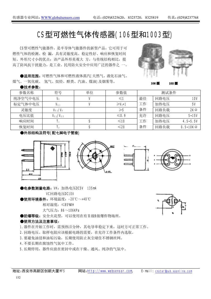 CS型可燃性气体传感器(106型和1003型)(传感器资料).pdf
 一种基于PWM的电压输出DAC电路设计.pdf
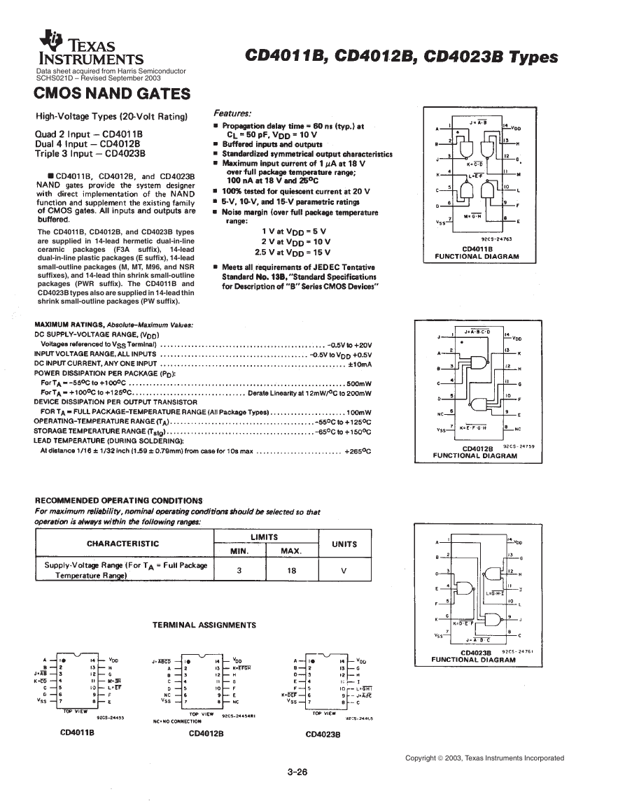 cd4011b(智能车电机驱动).pdf
 电路设计规范_中兴.pdf
 HA50-P(传感器资料).pdf
 ETD-core(TDK磁芯资料).pdf
 Po188-c[1](传感器资料).pdf