Document Number: MMA7660FC
Rev 1, 3/2009
MMA7660FC
MMA7660FC: XYZ-AXIS
ACCELEROMETER
±1.5 g
Bottom View
10 LEAD
DFN
CASE 2002-03
Top View
RESERVED
N/C
AVDD
AVSS
INT
1
2
3
4
5
10
N/C
9
8
7
6
DVDD
DVSS
SDA
SCL
Figure 1. Pin Connections
Freescale Semiconductor
Technical Data
3-Axis Orientation/Motion
Detection Sensor
The MMA7660FC is a ±1.5 g 3-Axis Accelerometer with Digital Output
(I2C). It is a very low power, low profile capacitive MEMS sensor
featuring a low pass filter, compensation for 0g offset and gain errors,
and conversion to 6-bit digital values at a user configurable samples
per second. The device can be used for sensor data changes, product
orientation, and gesture detection through an interrupt pin (INT). The
device is housed in a small 3mm x 3mm x 0.9mm DFN package.
Features
• Digital Output (I2C)
•
•
3mm x 3mm x 0.9mm DFN Package
Low Power Current Consumption: Off Mode: 0.4 µA,
Standby Mode: 3 µA, Active Mode: 47 µA at 1 ODR
• Configurable Samples per Second from 1 to 120 samples a second.
•
Low Voltage Operation:
– Analog Voltage: 2.4 V - 3.6 V
– Digital Voltage: 1.71 V - 3.6 V
Tilt Orientation Detection for Portrait/Landscape Capability
• Auto-Wake/Sleep Feature for Low Power Consumption
•
• Gesture Detection Including Shake Detection and Tap Detection
• Robust Design, High Shocks Survivability (10,000 g)
• RoHS Compliant
• Halogen Free
• Environmentally Preferred Product
•
Low Cost
Typical Applications
• Mobile Phone/ PMP/PDA: Orientation Detection (Portrait/Landscape),
Image Stability, Text Scroll, Motion Dialing, Tap to Mute
Laptop PC: Anti-Theft
•
• Gaming: Motion Detection, Auto-Wake/Sleep For Low Power
Consumption
• Digital Still Camera
ORDERING INFORMATION
Part Number
Temperature Range
Package
Shipping
MMA7660FCT
–40 to +85°C
MMA7660FCR1
–40 to +85°C
DFN-10
DFN-10
Tray
7” Tape & Reel
This document contains certain information on a new product.
Specifications and information herein are subject to change without notice.
© Freescale Semiconductor, Inc., 2009. All rights reserved.
�
Contents
ELECTRO STATIC DISCHARGE (ESD) ...................................................................................................................................... 6
PRINCIPLE OF OPERATION ...................................................................................................................................................... 8
MODES OF OPERATION ............................................................................................................................................................ 9
CONFIGURABLE SAMPLES PER SECONDS AND INTERRUPT SETTINGS ......................................................................... 10
POWER SAVING FEATURES ................................................................................................................................................... 10
TESTING THE LOGIC CHAIN ................................................................................................................................................... 10
FEATURES ................................................................................................................................................................................ 10
Tap Detection ...................................................................................................................................................................... 11
Shake Detection .................................................................................................................................................................. 12
Auto-Wake/Sleep ................................................................................................................................................................ 12
REGISTER DEFINITIONS ......................................................................................................................................................... 13
SERIAL INTERFACE ................................................................................................................................................................. 20
Serial-Addressing ................................................................................................................................................................ 20
Start and Stop Conditions ................................................................................................................................................... 20
Bit Transfer .......................................................................................................................................................................... 20
Acknowledge ....................................................................................................................................................................... 21
The Slave Address .............................................................................................................................................................. 21
Message Format for Writing MMA7660FC .......................................................................................................................... 21
Message Format for Reading MMA7660FC ........................................................................................................................ 22
APPENDIX A – PACKAGE REQUIREMENTS FOR MMA7660FC ............................................................................................ 23
Minimum Recommended Footprint for Surface Mounted Applications ............................................................................... 23
Soldering And Mounting Guidelines for the DFN Accelerometer Sensor to a PC Board .................................................... 23
Overview of Soldering Considerations ................................................................................................................................ 23
Halogen Content ................................................................................................................................................................. 23
PCB Mounting Recommendations ...................................................................................................................................... 23
APPENDIX B - SENSING DIRECTION ...................................................................................................................................... 25
APPENDIX C - MMA7660FC ACQUISITION CODE TABLE ..................................................................................................... 26
Sensors
Freescale Semiconductor
MMA7660FC
2
�
List of Tables
Pin Description . . . . . . . . . . . . . . . . . . . . . . . . . . . . . . . . . . . . . . . . . . . . . . . . . . . . . . . . . . . . . . . . . . . . . . . . . . . . . . . . . . . . . . . 5
Maximum Ratings . . . . . . . . . . . . . . . . . . . . . . . . . . . . . . . . . . . . . . . . . . . . . . . . . . . . . . . . . . . . . . . . . . . . . . . . . . . . . . . . . . . . . 6
ESD And Latch-up Protection Characteristics . . . . . . . . . . . . . . . . . . . . . . . . . . . . . . . . . . . . . . . . . . . . . . . . . . . . . . . . . . . . . . . 6
Operating Characteristics . . . . . . . . . . . . . . . . . . . . . . . . . . . . . . . . . . . . . . . . . . . . . . . . . . . . . . . . . . . . . . . . . . . . . . . . . . . . . . . 7
Modes Of Operation . . . . . . . . . . . . . . . . . . . . . . . . . . . . . . . . . . . . . . . . . . . . . . . . . . . . . . . . . . . . . . . . . . . . . . . . . . . . . . . . . . . 9
Feature Summary Table . . . . . . . . . . . . . . . . . . . . . . . . . . . . . . . . . . . . . . . . . . . . . . . . . . . . . . . . . . . . . . . . . . . . . . . . . . . . . . . 10
Orientation Detection Logic of when Interrupt will Occur . . . . . . . . . . . . . . . . . . . . . . . . . . . . . . . . . . . . . . . . . . . . . . . . . . . . . . 11
Auto Wake/Sleep Truth Table . . . . . . . . . . . . . . . . . . . . . . . . . . . . . . . . . . . . . . . . . . . . . . . . . . . . . . . . . . . . . . . . . . . . . . . . . . 12
User Register Summary . . . . . . . . . . . . . . . . . . . . . . . . . . . . . . . . . . . . . . . . . . . . . . . . . . . . . . . . . . . . . . . . . . . . . . . . . . . . . . . 13
Modes . . . . . . . . . . . . . . . . . . . . . . . . . . . . . . . . . . . . . . . . . . . . . . . . . . . . . . . . . . . . . . . . . . . . . . . . . . . . . . . . . . . . . . . . . . . . . 16
Sensors
Freescale Semiconductor
MMA7660FC
3
�
List of Figures
I2C Connection to MCU . . . . . . . . . . . . . . . . . . . . . . . . . . . . . . . . . . . . . . . . . . . . . . . . . . . . . . . . . . . . . . . . . . . . . . . . . . . . . . . . 5
Simplified Accelerometer Functional Block Diagram . . . . . . . . . . . . . . . . . . . . . . . . . . . . . . . . . . . . . . . . . . . . . . . . . . . . . . . . . . 5
Simplified Transducer Physical Model . . . . . . . . . . . . . . . . . . . . . . . . . . . . . . . . . . . . . . . . . . . . . . . . . . . . . . . . . . . . . . . . . . . . . 8
State Machine of Modes . . . . . . . . . . . . . . . . . . . . . . . . . . . . . . . . . . . . . . . . . . . . . . . . . . . . . . . . . . . . . . . . . . . . . . . . . . . . . . . . 9
2-Wire Serial Interface Timing Details . . . . . . . . . . . . . . . . . . . . . . . . . . . . . . . . . . . . . . . . . . . . . . . . . . . . . . . . . . . . . . . . . . . . 20
Start and Stop Conditions . . . . . . . . . . . . . . . . . . . . . . . . . . . . . . . . . . . . . . . . . . . . . . . . . . . . . . . . . . . . . . . . . . . . . . . . . . . . . . 20
Bit Transfer . . . . . . . . . . . . . . . . . . . . . . . . . . . . . . . . . . . . . . . . . . . . . . . . . . . . . . . . . . . . . . . . . . . . . . . . . . . . . . . . . . . . . . . . . 20
Acknowledge . . . . . . . . . . . . . . . . . . . . . . . . . . . . . . . . . . . . . . . . . . . . . . . . . . . . . . . . . . . . . . . . . . . . . . . . . . . . . . . . . . . . . . . 21
Slave Address . . . . . . . . . . . . . . . . . . . . . . . . . . . . . . . . . . . . . . . . . . . . . . . . . . . . . . . . . . . . . . . . . . . . . . . . . . . . . . . . . . . . . . 21
Single Byte Write . . . . . . . . . . . . . . . . . . . . . . . . . . . . . . . . . . . . . . . . . . . . . . . . . . . . . . . . . . . . . . . . . . . . . . . . . . . . . . . . . . . . 21
Multiple Bytes Write . . . . . . . . . . . . . . . . . . . . . . . . . . . . . . . . . . . . . . . . . . . . . . . . . . . . . . . . . . . . . . . . . . . . . . . . . . . . . . . . . . 22
Single Byte Read . . . . . . . . . . . . . . . . . . . . . . . . . . . . . . . . . . . . . . . . . . . . . . . . . . . . . . . . . . . . . . . . . . . . . . . . . . . . . . . . . . . . 22
Multiple Bytes Read . . . . . . . . . . . . . . . . . . . . . . . . . . . . . . . . . . . . . . . . . . . . . . . . . . . . . . . . . . . . . . . . . . . . . . . . . . . . . . . . . . 22
Package Footprint, PCB Land Pattern, and Stencil Design . . . . . . . . . . . . . . . . . . . . . . . . . . . . . . . . . . . . . . . . . . . . . . . . . . . . 24
PCB Land Pattern Detail . . . . . . . . . . . . . . . . . . . . . . . . . . . . . . . . . . . . . . . . . . . . . . . . . . . . . . . . . . . . . . . . . . . . . . . . . . . . . . 24
Product Orientation on Perpendicular Axis . . . . . . . . . . . . . . . . . . . . . . . . . . . . . . . . . . . . . . . . . . . . . . . . . . . . . . . . . . . . . . . . . 25
Product Orientations Showing Direction for Each Axis in Composite . . . . . . . . . . . . . . . . . . . . . . . . . . . . . . . . . . . . . . . . . . . . . 25
Sensors
Freescale Semiconductor
MMA7660FC
4
�
Top View
Table 1. Pin Description
Pin # Pin Name
Description
1 RESERVED Connect to AVSS
2
N/C
RESERVED
N/C
AVDD
AVSS
INT
1
2
3
4
5
10
N/C
9
8
7
6
DVDD
DVSS
SDA
SCL
Figure 1. .Pinout
VDD
C1
10 μf
C2
0.1 μf
1
2
3
4
5
RESERVED
N/C
AVDD
AVSS
INT
10
9
8
7
6
N/C
DVDD
DVSS
SDA
SCL
Pin
Status
Input
Input
Input
Input
Output
Input
Open
Drain
Input
Input
Input
3
4
5
6
7
8
9
10
AVDD
AVSS
INT
SCL
SDA
DVSS
DVDD
N/C
No Internal Connection, leave
unconnected or connect to Ground
Device Power
Device Ground
Interrupt/Data Ready
I2C Serial Clock
I2C Serial Data
Digital I/O Ground
Digital I/O Power
No Internal Connection,
recommended to connect to Ground
VDD
C3
10 μf
C4
0.1 μf
GND
MMA7660FC
VDD
GND
R1
4.70 K
R2
4.70 K
MCU
SDA
SCL
INT1
AVDD
DVDD
VSS
Figure 2. I2C Connection to MCU
INTERNAL
OSC
CLOCK
GEN
X-axis
Transducer
Y-axis
Transducer
Z-axis
Transducer
MUX
C-to-V
CONVERTER
AMP
ADC
I2C
OFFSET
TRIM
GAIN
TRIM
Figure 3. Simplified Accelerometer Functional Block Diagram
CONTROL LOGIC
Sensors
Freescale Semiconductor
SDA
SCL
INT
MMA7660FC
5
�
Table 2. Maximum Ratings
(Maximum ratings are the limits to which the device can be exposed without causing permanent damage.)
Rating
Maximum Acceleration (all axes, 100 μs)
Analog Supply Voltage
Digital I/O pins Supply Voltage
Drop Test
Storage Temperature Range
Symbol
gmax
AVDD
DVDD_IO
Ddrop
Tstg
Value
10,000
-0.3 to +3.6
-0.3 to +3.6
1.8
-40 to +125
Unit
g
V
V
m
°C
ELECTRO STATIC DISCHARGE (ESD)
WARNING: This device is sensitive to electrostatic discharge.
Although the Freescale accelerometer contains internal 2000 V ESD protection circuitry, extra precaution must be taken by
the user to protect the chip from ESD. A charge of over 2000 V can accumulate on the human body or associated test equipment.
A charge of this magnitude can alter the performance or cause failure of the chip. When handling the accelerometer, proper ESD
precautions should be followed to avoid exposing the device to discharges which may be detrimental to its performance.
Table 3. ESD And Latch-up Protection Characteristics
Rating
Human Body Model
Machine Model
Charge Device Model
Latch-up current at TA = 85°C
Symbol
HBM
MM
CDM
Value
±2000
±200
±500
±100
Unit
V
V
V
mA
Sensors
Freescale Semiconductor
MMA7660FC
6
�
Table 4. Operating Characteristics
Unless otherwise noted: -40°C < TA < 85°C, 2.4 V < AVDD < 3.6 V, 1.71 V < DVDD < 3.6 V, Acceleration = 0g
Typical values are at AVDD = 2.8 V, DVDD = 2.8 V, TA = +25°C
Characteristics
Analog Supply Voltage
Standby/Operation Mode
Enable Bus Modeon Mode
Digital I/O Pins Supply Voltage
Standby/Operation Mode
Enable Bus Modeon Mode
Supply Current Drain
Off Mode
Power Down Mode
Standby Mode
Active Mode, ODR = 1
Active Mode, ODR = 2
Active Mode, ODR = 4
Active Mode, ODR = 8
Active Mode, ODR = 16
Active Mode, ODR = 32
Active Mode, ODR = 64
Active Mode, ODR = 120
Operating Temperature Range
0g Output Signal (TA = 25°C, AVDD = 2.8 V)
0g offset ±1.5g range
0g offset Temperature Variation
Sensitivity (TA = 25°C, AVDD = 2.8 V)
±1.5g range (25°C) 6 bit
Acceleration Sensitivity at TAMB
Acceleration Sensitivity Temperature Variation
Input High Voltage
Input Low Voltage
Output Low Voltage (IOL = 6 mA + SDA, INT)
Input Leakage Current
Internal Clock Frequency (TA = 25°C, AVDD = 2.8 V)
I2C Interface Speed
Control Timing
Turn on time from AVDD = 0 V to AVDD = 2.5 V
Turn off time from Active to Standby Mode
Turn on time Standby to Active Mode
Timing Clock Source Accuracy (TA = 25°C, DVDD = 1.8 V)
Timing Clock Source Temperature Variation
Symbol
AVDD
AVDD
DVDD_IO
DVDD_IO
IDD
IDD
IDD
IDD
IDD
IDD
IDD
IDD
IDD
IDD
IDD
TA
VOFF
VIH
VIL
VOL
IIH, IIL
tCLK
Min
2.4
1.71
1.71
0
38
37
48
59
70
85
170
224
-40
-3
-8
0.7 x DVDD
135
-10
-15
Typ
2.8
0
2.8
1.8
0.4
2
2
47
49
54
66
89
133
221
294
25
0
±2.5
21.33
1
0.025
150
Max
3.6
AVDD
3.6
10
62
60
83
86
100
171
262
350
85
3
8
0.35 x DVDD
0.5
165
400
1
1
1/ODR
10
15
Cross Axis Sensitivity
Noise(2)
Notes
1. Limits verified by characterization, not tested in production.
2. Noise is defined as quantiles given to a sample size. These are the occurrences of noise: 94% = ±1 count, 5% = ±2 counts, and 1% = ±3
1.01
±1
counts.
Unit
V
V
V
V
µA
µA
µA
µA
µA
µA
µA
µA
µA
µA
µA
°C
counts
mg/°C
count/g
%
mg/°C
V
µA
kHz
kHz
ms
ms
S
%
%
%
count
Sensors
Freescale Semiconductor
MMA7660FC
7
�
PRINCIPLE OF OPERATION
The Freescale Accelerometer consists of a MEMS capacitive sensing g-cell and a signal conditioning ASIC contained in a
single package. The sensing element is sealed hermetically at the wafer level using a bulk micro machined cap wafer. The
g-cell is a mechanical structure formed from semiconductor materials (polysilicon) using masking and etching processes.
The sensor can be modeled as a movable beam that moves between two mechanically fixed beams (Figure 4). Two gaps are
formed; one being between the movable beam and the first stationary beam and the second between the movable beam and the
second stationary beam.
The ASIC uses switched capacitor techniques to measure the g-cell capacitors and extract the acceleration data from the
difference between the two capacitors. The ASIC also signal conditions and filters (switched capacitor) the signal, providing a
digital output that is proportional to acceleration.
ACCELERATION
Figure 4. Simplified Transducer Physical Model
Sensors
Freescale Semiconductor
MMA7660FC
8
�

.pdf-第1页.png")
.pdf-第2页.png")
.pdf-第3页.png")
.pdf-第4页.png")
.pdf-第5页.png")
.pdf-第6页.png")
.pdf-第7页.png")
.pdf-第8页.png")
 Meta大模型论文:The Llama 3 Herd of Models.pdf
 ACS0709(传感器资料).PDF
 495个C语言常见问题集.pdf
 CS型可燃性气体传感器(106型和1003型)(传感器资料).pdf
 一种基于PWM的电压输出DAC电路设计.pdf
 cd4011b(智能车电机驱动).pdf
 电路设计规范_中兴.pdf
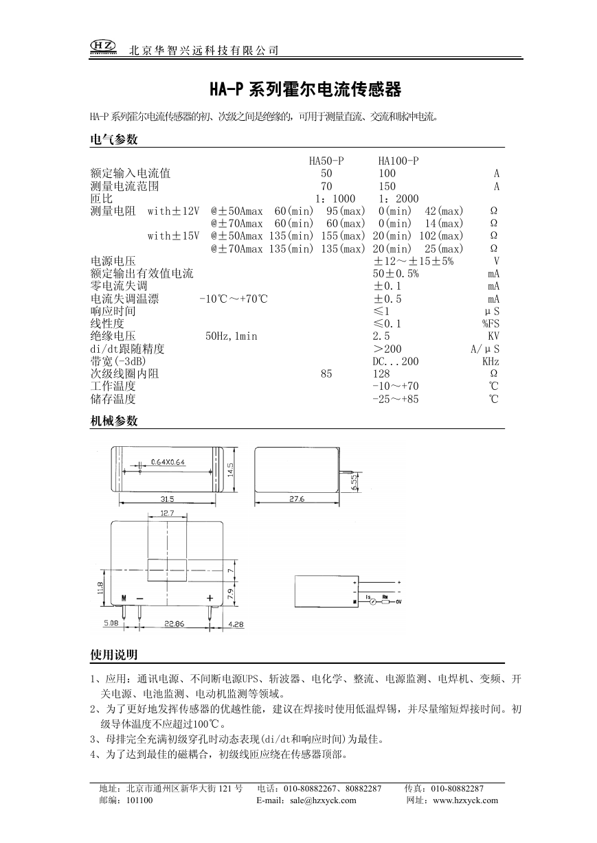 HA50-P(传感器资料).pdf
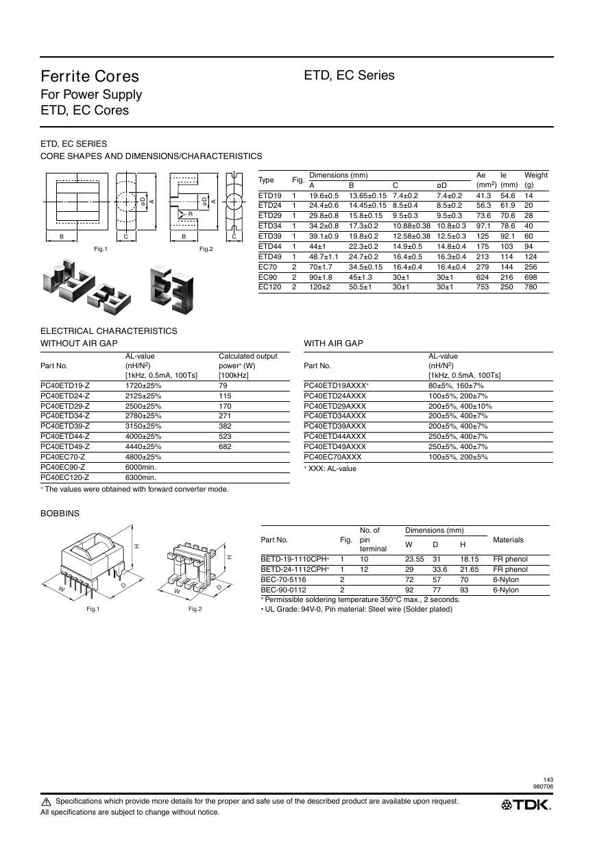 ETD-core(TDK磁芯资料).pdf