XM8A01M08V33A
XM8A51216V33A
January 2019
Selection Guide
Description
Maximum access time
Maximum operating current
Maximum CMOS standby current
Spec Unit
10/12
ns
75
35
mA
mA
8 Mbit (512K×16/1Mx8)
Asynchronous XRAM
Features
Asynchronous XRAM Memory
High speed access time
tAA = 10/12 ns
Low active power
ICC = 55 mA at 80 MHz
Low CMOS standby current
ISB2 = 20 mA (Typ)
Operating voltage range: 2.2 V to 3.6 V
Automatic power-down when deselected
TTL-compatible inputs and outputs
Available in 44-pin TSOP II, 48-pin TSOP I package
and 48-ball FBGA package
Functional Description
The XRAM is a new memory architecture designed to provide high-density and high-performance RAM at competitive price.
The XRAM uses advanced DRAM technology and self-refresh architecture to significantly improve the memory density,
performance and also simplify the user interface.
The XM8A51216V33A/XM8A01M08V33A XRAM, which is functionally equivalent to asynchronous SRAM, is a
high-performance, 8Mbits CMOS memory organized as 512K words by 16 bits and 1024K words by 8bits that supports an
asynchronous SRAM memory interface.
To write to the device, take Chip Enables (CE) and Write Enable (WE) input LOW. If Byte Low Enable (BLE) is LOW, then
data from I/O pins (DQ0 through DQ7), is written into the location specified on the address pins (A0 through A18). If Byte High
Enable (BHE) is LOW, then data from I/O pins (DQ8 through DQ15) is written into the location specified on the address pins
(A0 through A18). To read from the device, take Chip Enables (CE) and Output Enable (OE) LOW while forcing the Write
Enable (WE) HIGH. If Byte Low Enable (BLE) is LOW, then data from the memory location specified by the address pins
appears on DQ0 to DQ7. If Byte High Enable (BHE) is LOW, then data from memory appears on DQ8 to DQ15. See the Truth
Table on page 8 for a complete description of Read and Write modes.
The input or output pins (DQ0 through DQ15) are placed in a high impedance state when the device is deselected (CE), the
outputs are disabled (OE HIGH), the BHE and BLE are disabled (BHE, BLE HIGH), or during a write operation (CE and WE
LOW). A burst mode pin (MODE) defines the order of the burst sequence. When tied HIGH, the interleaved burst sequence is
selected. When tied LOW, the linear burst sequence is selected.
Note: Descriptions about BLE and BHE do not apply to XM8A01M08V33A XRAM.
*Products and specifications discussed herein are subject to change by XingMem without notice.
XingMem Technology Corporation Floor 11, Guoren Building, Nanshan District, Shenzhen, China +86-755-8633-6223
www.xingmem.com Document Number: 002-00008 Rev. A2 Revised Jan, 2019
�
Logic Block Diagram
XM8A01M08V33A
XM8A51216V33A
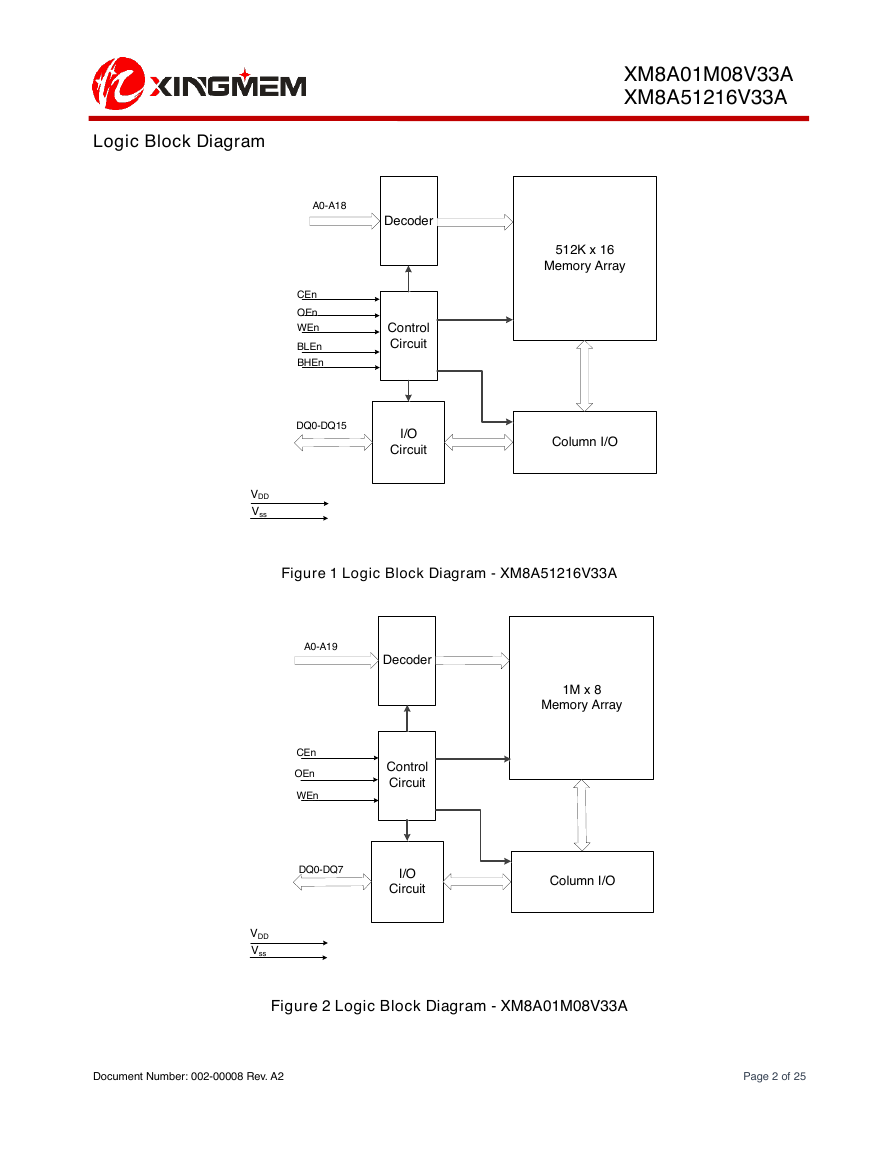
Figure 1 Logic Block Diagram - XM8A51216V33A
Figure 2 Logic Block Diagram - XM8A01M08V33A
Document Number: 002-00008 Rev. A2 Page 2 of 25
1M x 8Memory ArrayDecoderI/OCircuitA0-A19CEnOEnDQ0-DQ7VDDWEnControlCircuitColumn I/OVss512K x 16Memory ArrayDecoderI/OCircuitA0-A18CEnOEnWEnBLEnDQ0-DQ15VDDBHEnControlCircuitColumn I/OVss�
Contents
Features .................................................................. 1
Selection Guide ...................................................... 1
Functional Description .......................................... 1
Logic Block Diagram .............................................. 2
Pin Configurations ................................................. 4
Pin Definitions ......................................................... 8
Truth Table ............................................................... 8
Maximum Ratings ................................................... 9
Operating Range .................................................... 9
Electrical Characteristics ..................................... 10
Capacitance .......................................................... 11
XM8A01M08V33A
XM8A51216V33A
Thermal Resistance .............................................. 11
AC Test Loads and Waveforms ............................ 12
Switching Characteristics .................................... 13
Switching Waveforms ........................................... 14
Switching Waveforms (continued) ...................... 15
Ordering Information ............................................ 17
Ordering Code Definitions ................................... 19
Package Diagrams ................................................ 20
Acronyms .............................................................. 23
Document Conventions ........................................ 24
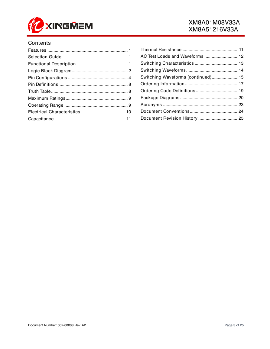
Document Revision History ................................. 25
Document Number: 002-00008 Rev. A2 Page 3 of 25
�
Pin Configurations
XM8A01M08V33A
XM8A51216V33A
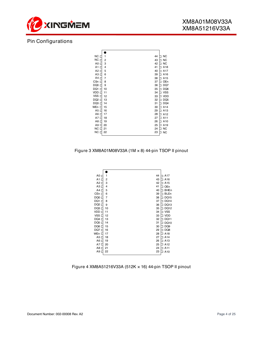
Figure 3 XM8A01M08V33A (1M × 8) 44-pin TSOP II pinout
Figure 4 XM8A51216V33A (512K × 16) 44-pin TSOP II pinout
Document Number: 002-00008 Rev. A2 Page 4 of 25
1324657981012111315141618171921202244424341394038363735333432303129272826242523NCNCA0A1A2A3A4CSnDQ0DQ1VDDVSSDQ2DQ3WEnA5A6A7A8A9NCNCNCNCNCA18A17A16A15OEnDQ7DQ6VSSVDDDQ5DQ4A14A13A12A11A10A19NCNC1324657981012111315141618171921202244424341394038363735333432303129272826242523A0A1A2A3A4CEnDQ0DQ1DQ2DQ3VDDVSSDQ4DQ5DQ6DQ7WEnA5A6A7A8A9A17A16A15OEnBHEnBLEnDQ15DQ14DQ13DQ12VSSVDDDQ11DQ10DQ9DQ8A18A14A13A12A11A10�
XM8A01M08V33A
XM8A51216V33A
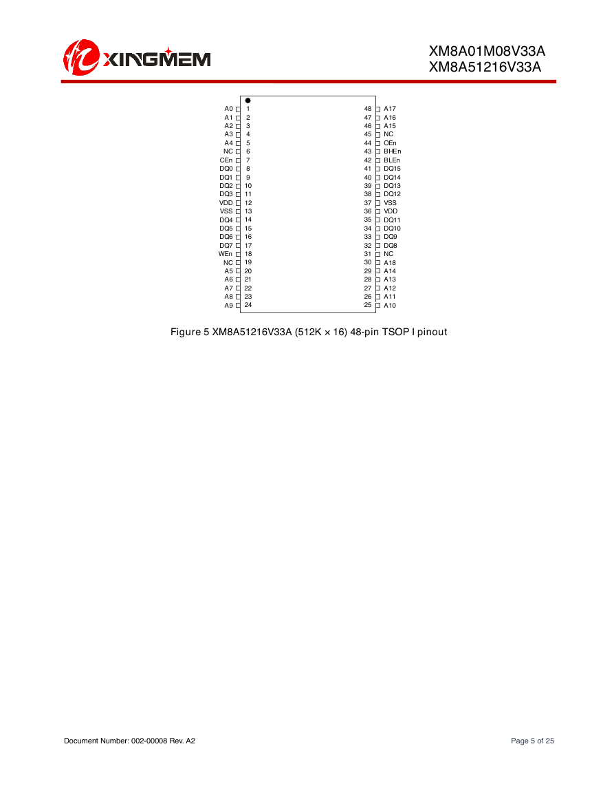
Figure 5 XM8A51216V33A (512K × 16) 48-pin TSOP I pinout
Document Number: 002-00008 Rev. A2 Page 5 of 25
132465798101211131514161817192120222423484647454344424041393738363435333132302829272526A0A1A2A3A4NCCEnDQ0DQ1DQ2DQ3VDDVSSDQ4DQ5DQ6DQ7WEnNCA5A6A7A8A9A17A16A15NCOEnBHEnBLEnDQ15DQ14DQ13DQ12VSSVDDDQ11DQ10DQ9DQ8NCA18A14A13A12A11A10�
XM8A01M08V33A
XM8A51216V33A
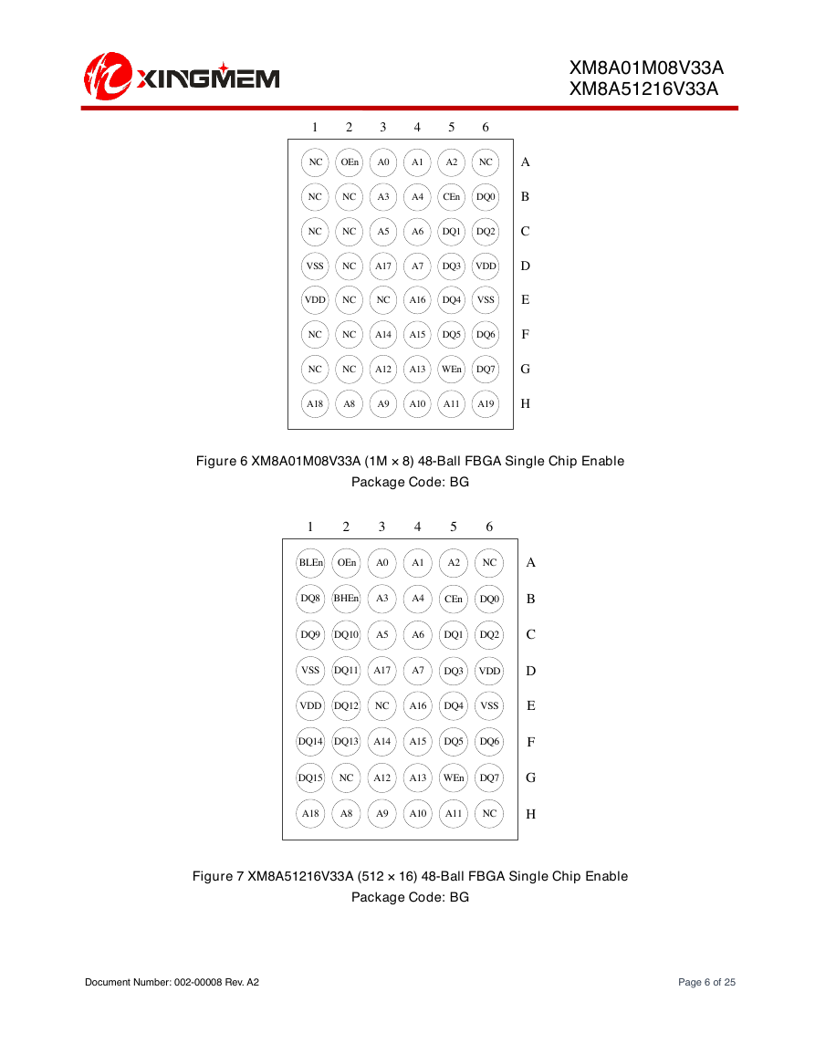
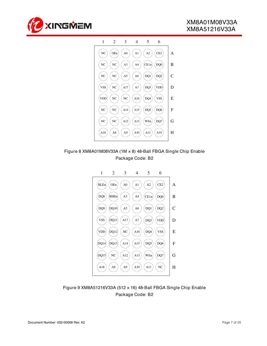
Figure 6 XM8A01M08V33A (1M × 8) 48-Ball FBGA Single Chip Enable
Package Code: BG
Figure 7 XM8A51216V33A (512 × 16) 48-Ball FBGA Single Chip Enable
Package Code: BG
Document Number: 002-00008 Rev. A2 Page 6 of 25
ACBDEFGH123456NCOEnA0A1A2NCA3A4A6A5A17A7A16A14A15A12A13A9A10A8A18NCA11NCCEnWEnVSSVDDVDDVSSA19DQ0DQ1DQ2DQ3DQ4DQ5DQ6DQ7NCNCNCNCNCNCNCNCNCACBDEFGH123456BLEnOEnA0A1A2NCA3A4A6A5A17A7A16A14A15A12A13A9A10A8A18NCA11BHEnCEnWEnVSSVDDVDDVSSNCDQ0DQ1DQ2DQ3DQ4DQ5DQ6DQ7DQ8DQ9DQ10DQ11DQ12NCDQ13DQ14DQ15�
XM8A01M08V33A
XM8A51216V33A
Figure 8 XM8A01M08V33A (1M × 8) 48-Ball FBGA Single Chip Enable
Package Code: B2
Figure 9 XM8A51216V33A (512 × 16) 48-Ball FBGA Single Chip Enable
Package Code: B2
Document Number: 002-00008 Rev. A2 Page 7 of 25
ACBDEFGH123456NCOEnA0A1A2CE2A3A4A6A5A17A7A16A14A15A12A13A9A10A8A18NCA11NCCE1nWEnVSSVDDVDDVSSA19DQ0DQ1DQ2DQ3DQ4DQ5DQ6DQ7NCNCNCNCNCNCNCNCNCACBDEFGH123456BLEnOEnA0A1A2CE2A3A4A6A5A17A7A16A14A15A12A13A9A10A8A18NCA11BHEnCE1nWEnVSSVDDVDDVSSNCDQ0DQ1DQ2DQ3DQ4DQ5DQ6DQ7DQ8DQ9DQ10DQ11DQ12NCDQ13DQ14DQ15�
XM8A01M08V33A
XM8A51216V33A
Pin Definitions
Name
VDD
VSS
BLEn, BHEn
A0-A19
CEn, CE1n, CE2
OEn
WEn
DQ0-DQ15
I/O
Supply
Supply
Input
Input
Input
Input
Input
I/O
Description
Power.
Ground.
Byte write enable signal, active LOW.
Address inputs.
Chip enable signal, active LOW.
Output enable signal, active LOW.
Write enable signal, active LOW.
Data inputs/outputs.
Note:
For all dual chip enable device, CEn represents the logical combination of CE1n and CE2. When CEn is LOW, CE1n is LOW, CE2 is HIGH. When CEn is HIGH, CE1n is
LOW or CE2 is HIGH.
Truth Table
The Truth Table for parts XM8A01M08V33A/XM8A51216V33A is as follows*.
Mode
WEn
BLEn
BHEn
CEn
OEn
DQ0-DQ7
DQ8-DQ15
Not Selected
Output Disabled
Read
Read
Read
Write
Write
Write
X
H
H
H
H
L
L
L
X
X
L
L
H
L
L
H
X
X
L
H
L
L
H
L
H
L
L
L
L
L
L
L
X
H
L
L
L
H
H
H
High-Z
High-Z
High-Z
High-Z
Data Out
Data Out
High-Z
Data Out
Data Out
Data In
Data In
High-Z
High-Z
Data In
High-Z
Data In
Note:
Descriptions about BLEn and BHEn do not apply to XM8A01M08V33A XRAM.
Document Number: 002-00008 Rev. A2 Page 8 of 25
�

