Application Note AN040
Folded dipole antenna for CC2400, CC2420, CC2430, CC2431,
and CC2480
By G. E. Jonsrud
1 KEYWORDS
• Radiation Pattern
• Line of sight range
• CC2400
• CC2420
2
INTRODUCTION
This application note describes the design
of a folded dipole antenna for CC2400,
CC2420, CC2430, CC2431, and CC2480.
The CC2400 is a true single-chip, general-
purpose transceiver for the 2.4 GHz SRD
band for data rates up to 1 Mbps. The
CC2420 is a true single-chip RF trans-
ceiver designed for low power wireless
networks operating in the 2.4 GHz SRD
band compliant with the ZigBee™/IEEE
802.15.4 standard. CC2430 is a true SoC
combining the CC2420 with a single cycle
8051 microcontroller. CC2431 is CC2430
with location engine. The CC2480 is a
cost-effective, low power, Z-Accel ZigBee
Processor
full ZigBee
functionality with a minimal development
effort.
The design described in this application
note is based on the CC2400, but it is
possible to tune the antenna impedance
so it can be used with CC2420, CC2430,
that provides
• CC2430
• CC2431
• CC2480
• Folded dipole
CC2431, and CC2480. The tuning is done
by adjusting the value of the inductor
placed across the RF pins.
The RF front end consists of three pin
connections. Two pins serve as a
differential interface shared by the LNA
and PA. The third pin changes voltage
level in order to provide power to the PA
during transmission and ground to the
LNA during
reception. A differential
interface provides a better utilisation of the
available supply voltage as well as less
parasitic capacitance to ground.
Design criteria for the antenna and the
design process are described. Also
included are test results and a comparison
of the tested antenna to a balun and
monopole antenna solution. Gerber files
and schematics can be downloaded from
www.ti.com/lpw.
SWRA093D
Page 1 of 26
�
Application Note AN040
Table of Contents
KEYWORDS ................................................................................................................... 1
1
INTRODUCTION............................................................................................................. 1
2
ABBREVIATIONS........................................................................................................... 3
3
DESIGN CRITERIA......................................................................................................... 4
4
DESIGN DESCRIPTION................................................................................................. 4
5
SCHEMATICS AND LAYOUT........................................................................................ 5
6
7
TUNING........................................................................................................................... 8
TEST RESULTS ........................................................................................................... 10
8
8.1 SUMMARY OF RESULTS............................................................................................ 13
9
CONCLUSION .............................................................................................................. 13
10 APPENDIX A - RADIATION DIAGRAMS .................................................................... 14
11 DOCUMENT HISTORY ................................................................................................ 26
SWRA093D
Page 2 of 26
�
Application Note AN040
3 ABBREVIATIONS
CC243x
CC2480
DC
EB
EIRP
EM
CC2400EM
FCC
FR4
FSK
ISM
LNA
PA
PCB
RBW
RF
RFC
SMA
SRD
VBW
CC2430 and CC2431
Z-Accel ZigBee Processor
Direct Current
Evaluation Board
Effective Isotropic Radiated Power
Electromagnetic
CC2400 Evaluation Module
Federal Communications Commission
Common PCB material
Frequency Shift Keying
Industrial Scientific and Medical
Low Noise Amplifier
Power Amplifier
Printed Circuit Board
Resolution Bandwidth
Radio Frequency
Radio Frequency Choke
Common RF connector
Short Range Device
Video Bandwidth
SWRA093D
Page 3 of 26
�
Application Note AN040
4 DESIGN CRITERIA
The following design criteria were important for the antenna design:
• Optimum load impedance for CC2400, 110 + j130 Ohm, differential
• DC-connection between RF pins and TXRX_switch pin
• TXRX_switch pin isolated from RF
• Few components
• Manufacturability
• Low spurious emission
• Low losses
• Omnidirectionality
The optimum termination impedance is a trade-off between optimum source impedance for
the internal LNA and optimum load for the internal PA. The TXRX_switch pin level is 0 V in
receive mode to provide ground for the LNA and 1.8 V in transmit mode to provide the
required supply voltage to the PA. This pin should be isolated from the RF signals by using a
shunt capacitor and/or a series inductor (RFC).
Antennas that are electrically short compared to the wavelength tend to be sensitive to
component variations in the tuning network. Electrically small antennas may cause yield
problems or require individual tuning.
Pay special attention to the harmonic levels for operation in the 2.4 GHz SRD band. Both the
second and third harmonic will fall within restricted bands as defined by FCC part 15.
In typical SRD applications, it is desired that the antenna radiates equally in all directions, i.e.
that the antenna is omni directional.
A folded dipole is attractive because of its high impedance that makes it easier to match to
the optimum impedance for the CC2400. The theoretical impedance is 292 Ohm for a half
wavelength folded dipole. A shunt inductor should provide the inductive part of the optimum
load impedance while reducing the real part. The folded dipole is a metal loop that will
provide DC contact between the RF pins. In addition the mid point of the antenna is virtual
ground, meaning that a connection can be made to the TXRX_switch pin without distorting
antenna performance. The folded dipole is a resonant structure that should be less sensitive
to component variations and provide low losses. The radiation pattern of a folded dipole is
omni-directional in the plane normal to the antenna.
5 DESIGN DESCRIPTION
An initial investigation to check the feasibility of the design was performed using the Smith
chart. Plotting the 292 Ohm in the Smith chart and adding a 15 nH shunt inductor resulted in
115 + j141 Ohm.
The CC2400EM reference design was selected as the base for the design. The CC2400EM
is a radio module with balun and an SMA connector. The balun with the SMA connector is
designed to work with 50 Ohm unbalanced devices such as a ¼ wave antenna and most RF
instruments
The antenna was implemented on the PCB as part of the layout. The antenna was placed
relatively close to the CC2400 to keep the design compact.
SWRA093D
Page 4 of 26
�
Application Note AN040
The antenna design was simulated before the layout was made. The antenna was designed
using an EM simulator and the matching circuit was simulated using a linear simulator and S-
parameters from the EM simulation.
The first step in the simulation was to design a folded dipole on a FR4 PCB in front of a
ground plane of the same size as the CC2400EM. The length of the antenna was adjusted
until the impedance was 290 Ohm. The next step was to add feed lines with pads for a shunt
inductor and a transmission line to the virtual ground point of the antenna for DC connection
to the TXRX switch pin. The transmission line to the TXRX switch pin was connected to
ground during the simulations and was fitted with pads for a series inductor. The inductor
pads were defined as ports to make it easy to simulate with various inductors in the following
S-parameter simulations. Due to the PCB material and the ground plane, the antenna
became shorter than the theoretical half wavelength. Finally, the inductor values were
determined using a linear simulator, S-parameters from the antenna simulation and S-
parameters for the inductors.
6 SCHEMATICS AND LAYOUT
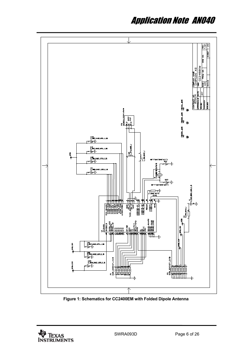
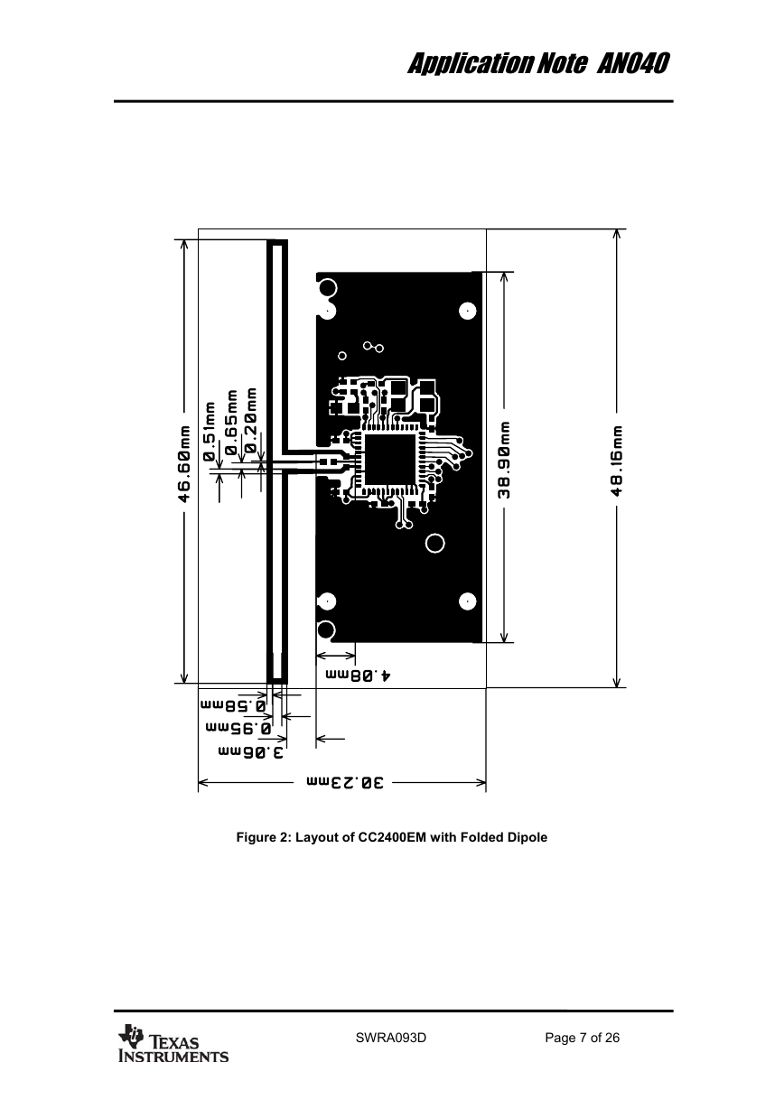
Figure 1 shows the schematic of the CC2400EM with the folded dipole antenna. Figure 2
shows the board layout. The distance to the antenna and extension of the ground plane
behind the antenna are critical parameters. If the PCB is wider than the CC2400EM board,
the ground plane, components and tracks should be pulled away from the end points of the
antenna.
SWRA093D
Page 5 of 26
�
Application Note AN040
Figure 1: Schematics for CC2400EM with Folded Dipole Antenna
SWRA093D
Page 6 of 26
�
Application Note AN040
Figure 2: Layout of CC2400EM with Folded Dipole
SWRA093D
Page 7 of 26
�
Application Note AN040
7 TUNING
The schematic in Figure 1 shows the recommended component values when matching the
antenna to CC2400. Since the optimum impedance of CC2420, CC243x, and CC2480 is
different from CC2400 is it required to tune the value of the matching inductor (L62) to obtain
optimum performance when implementing the antenna with these parts. The optimum load
impedance for CC2420, CC243x, and CC2480 is given in the data sheets. The size of the
ground plane, encapsulation of the board and objects in the vicinity of the antenna will also
affect the performance. Thus, it is important to have the antenna implemented in the
environment it is going to be used when performing the tuning. It might also be needed to
tune the length of the antenna to obtain optimum performance. The length of the antenna will
affect the resonance frequency. Implementations with ground plane size different from the
reference design and with encapsulation will most likely require slightly different antenna
length to ensure optimum performance in the middle of the 2.4 GHz ISM band. To find the
optimum length, test software that steps a carrier across the frequency band can be used.
Measuring the radiated power by using max hold on a spectrum analyzer will identify the
optimum frequency. If the frequency with highest radiation is too low, the antenna could be
made slightly shorter and if the maximum radiation is at a too high frequency, the antenna
should be made longer. Tuning of the antenna length could be done using a sharp knife and
soldering on copper tape or a small wire.
The purpose of tuning the value of L62 is to maximise output power while maintaining good
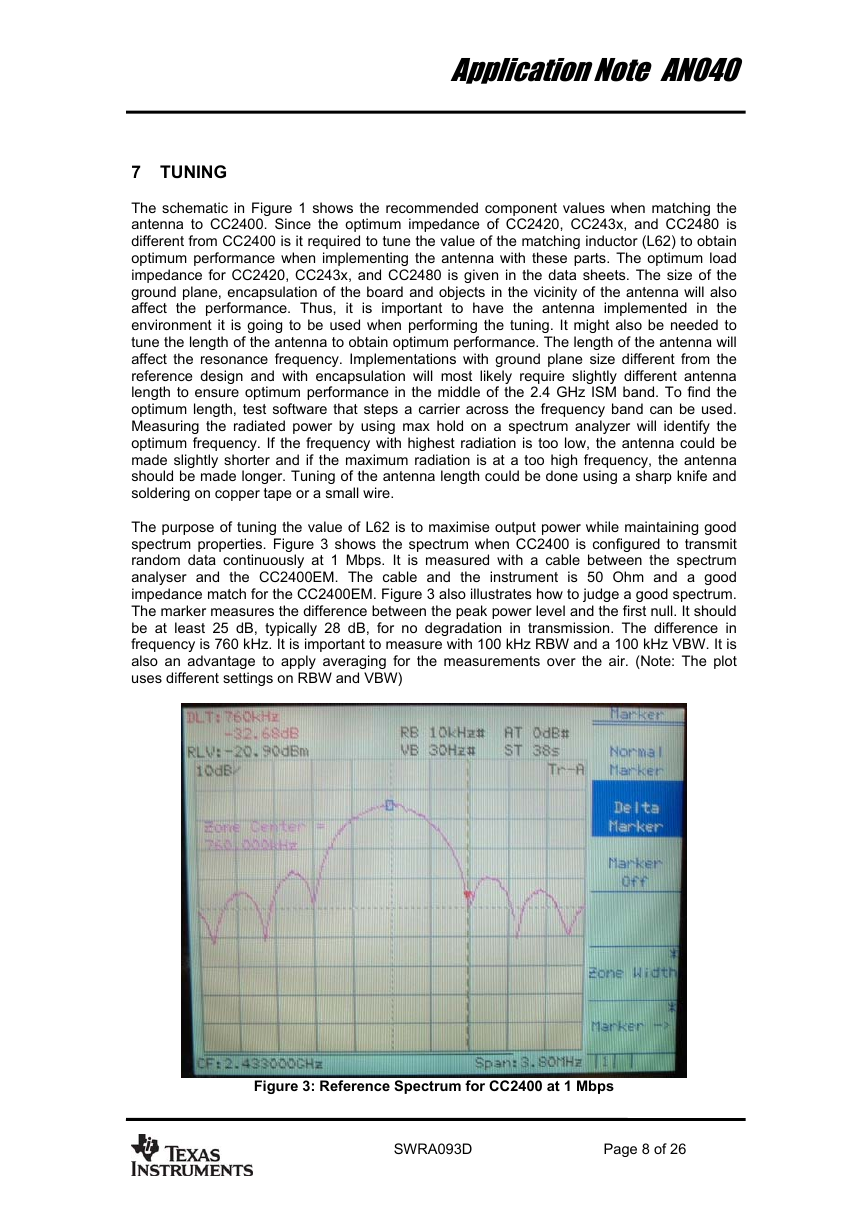
spectrum properties. Figure 3 shows the spectrum when CC2400 is configured to transmit
random data continuously at 1 Mbps. It is measured with a cable between the spectrum
analyser and the CC2400EM. The cable and the instrument is 50 Ohm and a good
impedance match for the CC2400EM. Figure 3 also illustrates how to judge a good spectrum.
The marker measures the difference between the peak power level and the first null. It should
be at least 25 dB, typically 28 dB, for no degradation in transmission. The difference in
frequency is 760 kHz. It is important to measure with 100 kHz RBW and a 100 kHz VBW. It is
also an advantage to apply averaging for the measurements over the air. (Note: The plot
uses different settings on RBW and VBW)
Figure 3: Reference Spectrum for CC2400 at 1 Mbps
SWRA093D
Page 8 of 26
�
