Small Size 2.4 GHz PCB antenna
Application Note AN043
By Audun Andersen
1 KEYWORDS
• CC25xx
• CC24xx
• CC2480
• PCB antenna
2
INTRODUCTION
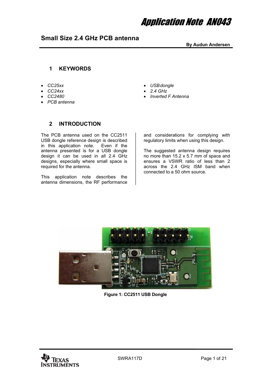
The PCB antenna used on the CC2511
USB dongle reference design is described
in this application note. Even if the
antenna presented is for a USB dongle
design it can be used in all 2.4 GHz
designs, especially where small space is
required for the antenna.
This application note describes
the
antenna dimensions, the RF performance
• USB dongle
• 2.4 GHz
•
Inverted F Antenna
for complying with
and considerations
regulatory limits when using this design.
The suggested antenna design requires
no more than 15.2 x 5.7 mm of space and
ensures a VSWR ratio of less than 2
across the 2.4 GHz ISM band when
connected to a 50 ohm source.
Figure 1: CC2511 USB Dongle
SWRA117D
Page 1 of 21
�
Application Note AN043
Table of Contents
1
2
3
4
KEYWORDS ................................................................................................................... 1
INTRODUCTION............................................................................................................. 1
ABBREVIATIONS........................................................................................................... 2
ANTENNA DESIGN........................................................................................................ 3
DESIGN GOALS.......................................................................................................... 3
SIMULATION............................................................................................................... 3
LAYOUT AND IMPLEMENTATION ................................................................................... 4
TEST RESULTS ............................................................................................................. 5
REFLECTION .............................................................................................................. 5
RADIATION PATTERN.................................................................................................. 7
OUTPUT POWER ...................................................................................................... 15
SPURIOUS EMISSION AND HARMONICS...................................................................... 17
CONCLUSION .............................................................................................................. 20
GENERAL INFORMATION .......................................................................................... 21
DOCUMENT HISTORY................................................................................................ 21
5
6
7
4.1
4.2
4.3
5.1
5.2
5.3
5.4
7.1
3 ABBREVIATIONS
Computer Aided Design
CC2400, CC2420, CC2430 and CC2431
CC2500, CC2510, CC2511, CC2550 and CC2520
Z-Accel ZigBee Processor
Inverted F Antenna
Industrial, Scientific and Medical
Line Of Sight
Printed Circuit Board
Packet Error Rate
Voltage Standing Wave Ratio
CAD
CC24xx
CC25xx
CC2480
IFA
ISM
LOS
PCB
PER
VSWR
SWRA117D
Page 2 of 21
�
Application Note AN043
4 ANTENNA DESIGN
The PCB antenna on the CC2511 USB dongle reference design is a meandered Inverted F
Antenna (IFA). The IFA was designed to match an impedance of 50 ohm at 2.45 GHz. Thus
no additional matching components are necessary.
4.1 Design Goals
The reflection at the feed point of the antenna determines how much of the applied power is
delivered to the antenna. A reflection of less than -10 dB across the 2.4 GHz ISM band, when
connected to a 50 ohm source, was a design goal. Reflection of less than -10 dB, or VSWR
less than 2, ensures that more than 90% of the available power is delivered to the antenna.
Bandwidth is in this document defined as the frequency band where more than 90% of the
available power is delivered to the antenna. Another design goal was to fit the size of the PCB
antenna on a USB dongle and to obtain good performance also when the dongle is
connected to a computer.
4.2 Simulation
IE3D from Zeland, which is an electromagnetic simulation tool, was used to design the
antenna. The accuracy of the simulation is controlled by the mesh. An increase of the mesh
increases the simulation time. Thus, for initial simulations mesh = 1 should be used. When a
fairly good result is achieved a higher mesh should be used to obtain more accurate results.
Comparison of simulation and measurement results shows that the measured reflection is
between the result obtained with mesh = 5 and mesh = 1; see Figure 2 for details.
Figure 2: Comparison of Simulation and Measurements Results
SWRA117D
Page 3 of 21
�
Application Note AN043
4.3 Layout and Implementation
Small changes of the antenna dimensions may have large impact on the performance.
Therefore it is strongly recommended to make an exact copy of the reference design to
achieve optimum performance. The easiest way to implement the antenna is to import the
gerber or DXF file showing the antenna layout. These files are named IFA_USB.spl and
IFA_USB.dxf respectively and are included in the CC2511 USB dongle reference design
available from http://www.ti.com\lpw. The imported file can be used as a template when
drawing the antenna. By using this procedure it should be possible to make an exact copy. If
the PCB CAD tool being used does not support import of DXF or gerber files, Figure 3 and
Table 1 should be used to ensure correct implementation. It is recommended to generate a
gerber file for comparison with IFA_USB.spl when making a manual implementation. Most
gerber viewers have the possibility to import several gerber files at the same time. Thus by
placing the gerber file, showing the manually implemented antenna, on top of IFA_USB.spl it
is easy to verify that the antenna is correctly implemented. It is also recommended to use the
same thickness and type of PCB material as used in the reference design. Information about
the PCB can be found in a separate readme file included in the reference design. To
compensate for a thicker/thinner PCB the antenna could be made slightly shorter/longer.
Figure 3: Antenna Dimensions
L1
L2
L3
L4
L5
L6
W1
W2
D1
D2
D3
D4
D5
D6
3.94 mm
2.70 mm
5.00 mm
2.64 mm
2.00 mm
4.90 mm
0.90 mm
0.50 mm
0.50 mm
0.30 mm
0.30 mm
0.50 mm
1.40mm
1.70 mm
Table 1: Antenna Dimensions
SWRA117D
Page 4 of 21
�
Application Note AN043
5 TEST RESULTS
Reflection, radiation pattern and variation of output power across a wide frequency band were
measured to verify the performance of the PCB antenna. Measurements of the dongle in free
space and when connected to a laptop were performed to verify that the antenna is suitable
both for USB dongle designs and in a standalone application. Free space is in this document
interpreted as a measurement performed without connecting the dongle to a computer. In
such a measurement the dongle is only powered by a battery.
5.1 Reflection
All the reflection measurements were performed with a network analyzer connected to a
semi-rigid coax cable, which was soldered to the feed point of the antenna. Because of the
small size antenna and the small ground plane this kind of measurements is heavily affected
by the presence and placement of the coax cable. This influence can result in a small
uncertainty in resonance frequency and measured reflection. Typically different placement of
the semi-rigid coax cable could change the resonance frequency with 5 -10 MHz and the
reflection with 3 - 4 dB.
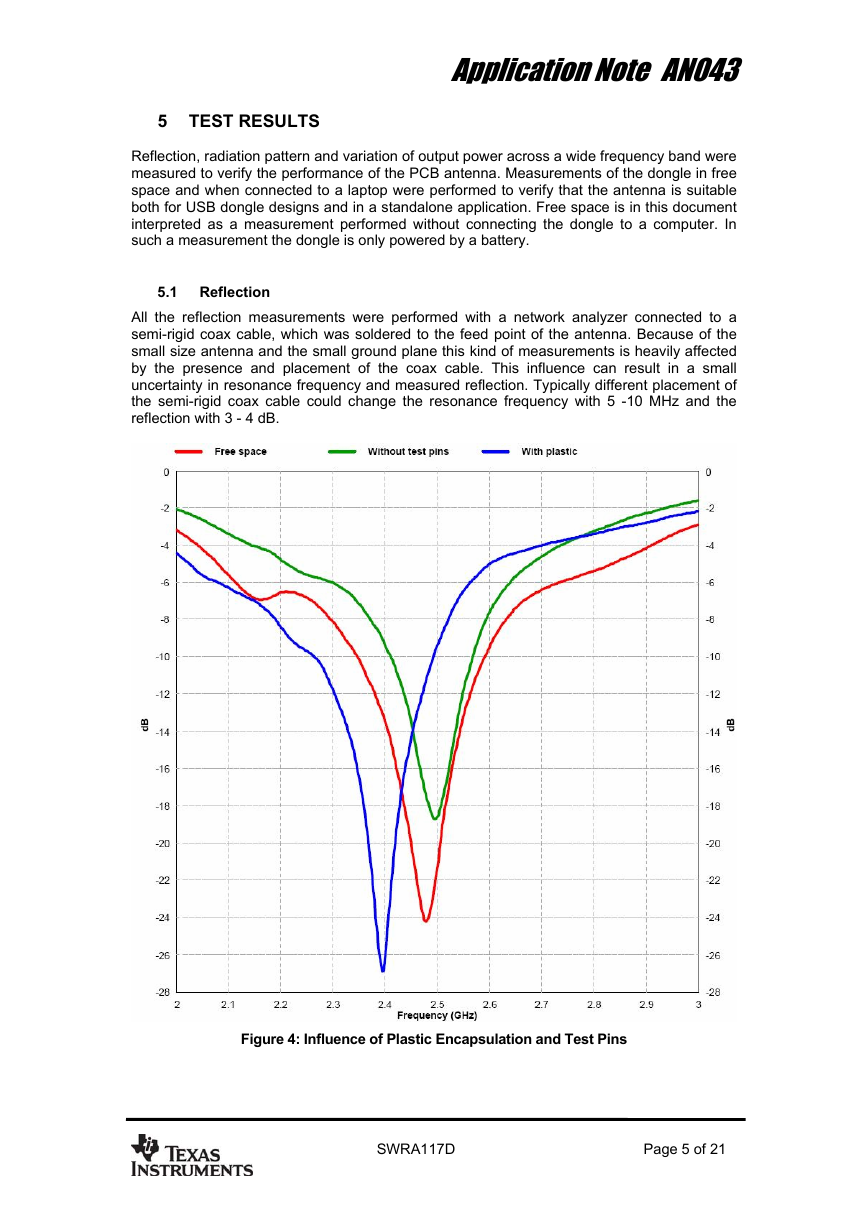
Figure 4: Influence of Plastic Encapsulation and Test Pins
SWRA117D
Page 5 of 21
�
Application Note AN043
A small part on the CC2511 USB dongle PCB is equipped with test pins. These are intended
for use during development. This part of the PCB will typically be omitted in a final application.
The red and green graph on Figure 4 shows that removing this part of the PCB has a small
impact on the performance. Figure 4 also shows that plastic encapsulation of the dongle will
shift the resonance frequency to a lower frequency. This can be compensated by making the
antenna slightly shorter.
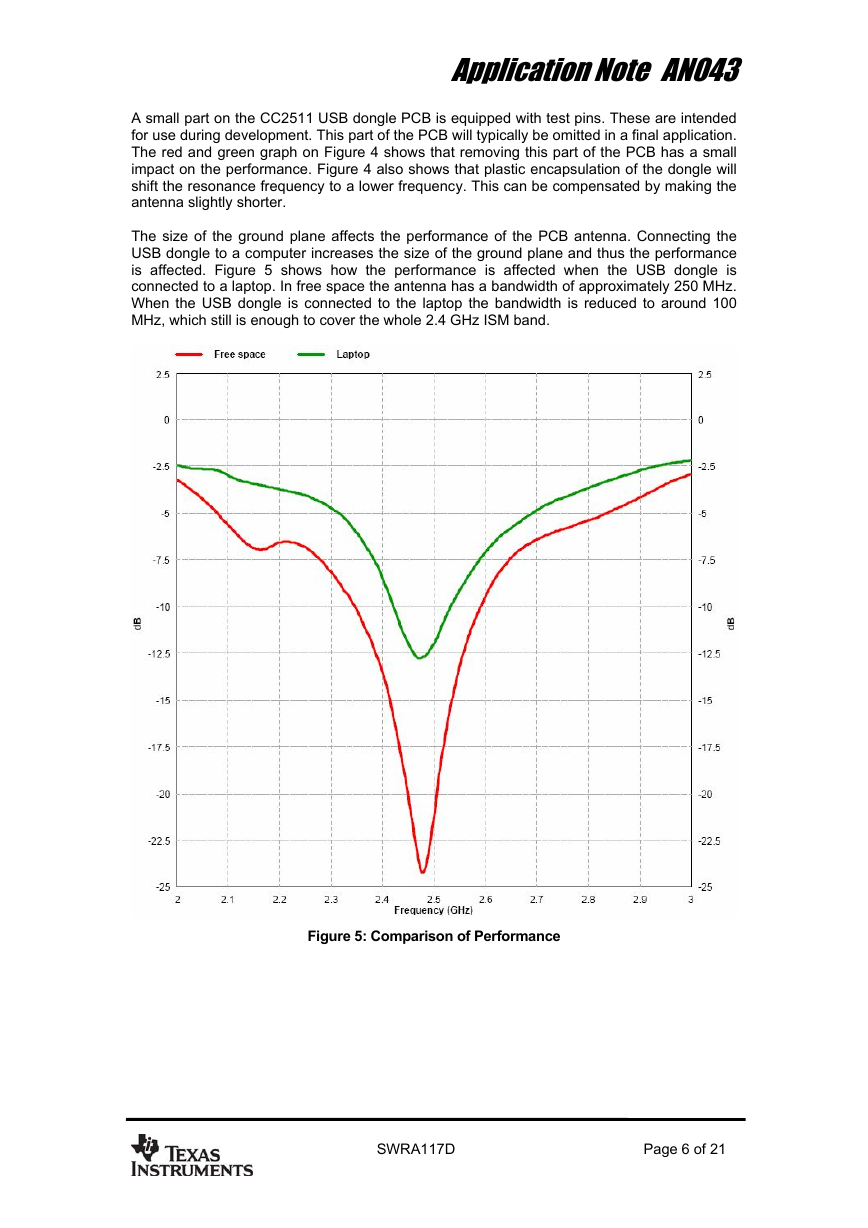
The size of the ground plane affects the performance of the PCB antenna. Connecting the
USB dongle to a computer increases the size of the ground plane and thus the performance
is affected. Figure 5 shows how the performance is affected when the USB dongle is
connected to a laptop. In free space the antenna has a bandwidth of approximately 250 MHz.
When the USB dongle is connected to the laptop the bandwidth is reduced to around 100
MHz, which still is enough to cover the whole 2.4 GHz ISM band.
Figure 5: Comparison of Performance
SWRA117D
Page 6 of 21
�
Application Note AN043
5.2 Radiation Pattern
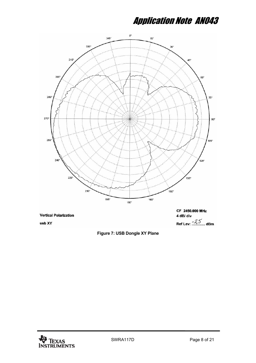
The radiation pattern for the antenna implemented on the CC2511 USB dongle reference
design has been measured in an anechoic chamber. Figure 7 through Figure 12 shows
radiation patterns for three planes, XY, XZ and YZ, measured with vertical and horizontal
polarization. All these measurement were performed without connecting the dongle to a
computer. Figure 13 and Figure 14 shows the radiation pattern when the dongle is connected
to a laptop. All measurements were performed with 0 dBm output power. Figure 6 shows how
the different radiation patters are related to the positioning of the antenna.
XY plane
YZ plane
XZ plane
Figure 6: How to Relate the Antenna to the Radiation Patterns
SWRA117D
Page 7 of 21
�
Application Note AN043
Figure 7: USB Dongle XY Plane
SWRA117D
Page 8 of 21
�
