Folded Dipole Antenna for CC25xx
Design Note DN004
By Audun Andersen
Keywords
• CC2500
• CC2550
• CC2510
• CC2511
1
Introduction
following products
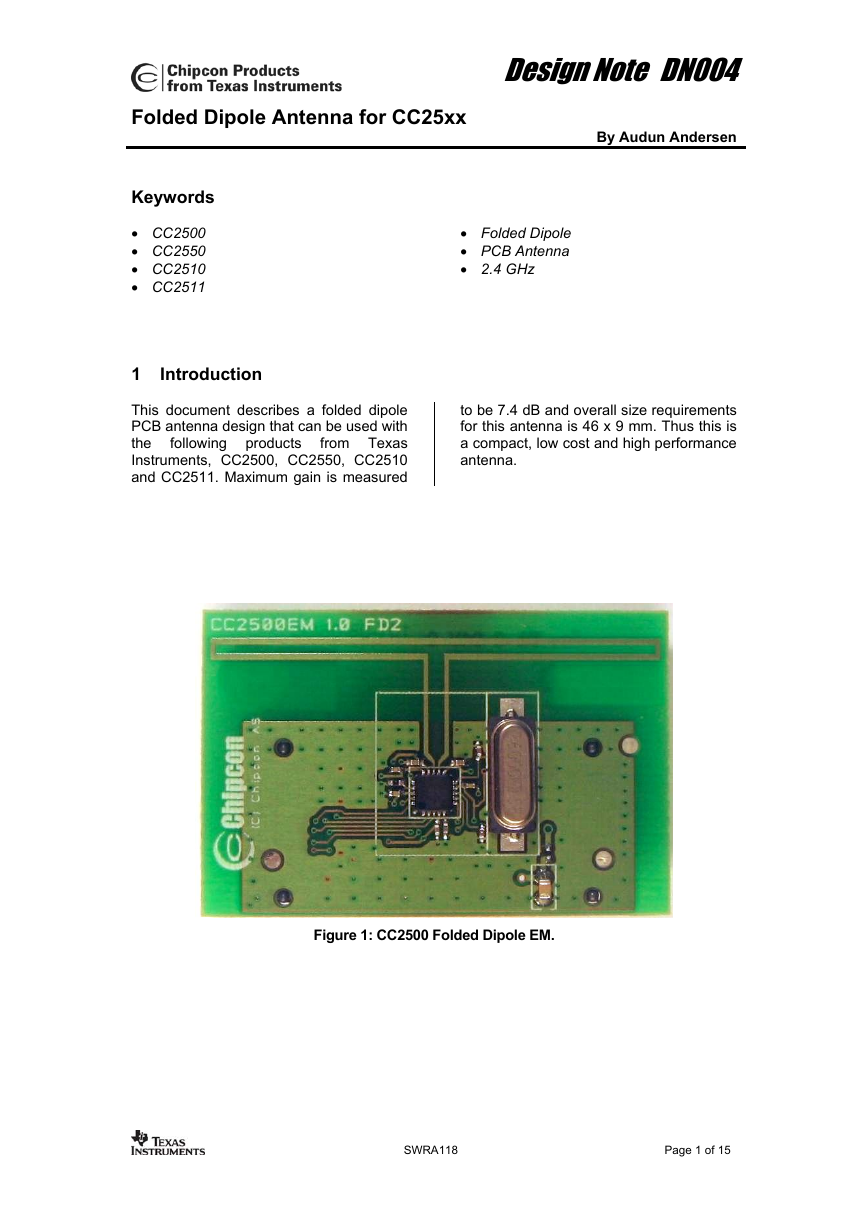
This document describes a folded dipole
PCB antenna design that can be used with
the
from Texas
Instruments, CC2500, CC2550, CC2510
and CC2511. Maximum gain is measured
• Folded Dipole
• PCB Antenna
• 2.4 GHz
to be 7.4 dB and overall size requirements
for this antenna is 46 x 9 mm. Thus this is
a compact, low cost and high performance
antenna.
Figure 1: CC2500 Folded Dipole EM.
SWRA118
Page 1 of 15
�
Table of Contents
Design Note DN004
KEYWORDS.............................................................................................................................. 1
1
INTRODUCTION............................................................................................................. 1
ABBREVIATIONS........................................................................................................... 2
2
DESCRIPTION OF THE FOLDED DIPOLE DESIGN .................................................... 3
3
IMPLEMENTATION OF THE FOLDED DIPOLE.................................................................... 3
4
RESULTS........................................................................................................................ 5
RADIATION PATTERN .................................................................................................. 5
BANDWIDTH............................................................................................................. 12
SPURIOUS AND HARMONIC EMISSION......................................................................... 13
CONCLUSION .............................................................................................................. 13
GENERAL INFORMATION .......................................................................................... 14
DOCUMENT HISTORY................................................................................................ 14
IMPORTANT NOTICE .................................................................................................. 15
3.1
4.1
4.2
4.3
6.1
5
6
7
2 Abbreviations
CC25xx
CAD
DXF
EM
LOS
PCB
CC2500, CC2550, CC2510, CC2511
Computer Aided Design
Data eXchange Format
Evaluation Module
Line Of Sight
Printed Circuit Board
SWRA118
Page 2 of 15
�
Design Note DN004
3 Description of the folded dipole design
Since the impedance of the folded dipole is matched directly to the impedance of the radio no
external matching components are needed. Dependent on which regulatory limits the
application should comply with, two filtering capacitors might however be needed. To ensure
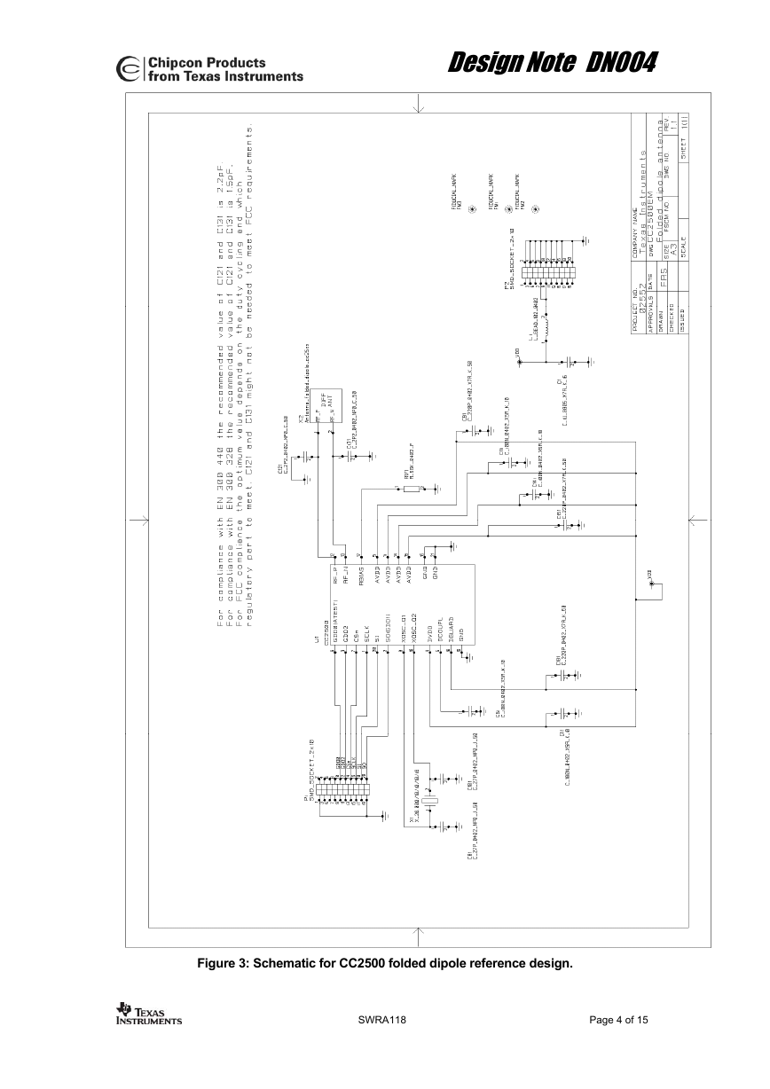
compliance with ETSI requirements for receiver spurious emission, C121 and C131 in Figure
3 must be included. The optimum value of C121 and C131 depends on which ETSI standard
to comply with. For EN 300 440, 2.2 pF is recommended and 1.5 pF is recommended for EN
300 328. The required filtering for compliance with FCC is dependent on which regulatory
part to meet, part 15.247 or 15.249, and the duty cycle of the transmitted signal. Including
C121 and C131 reduces the output power but ensures lower harmonic emission in TX and
reduced VCO leakage in RX. Typically a board with two 1.5 pF capacitors will have 2 dB less
output power than a board without C121 and C131.
file
is called
Implementation of the folded dipole
3.1
It is important to make an exact copy of the antenna dimensions to obtain optimum
performance. The easiest approach to implement the antenna in a PCB CAD tool is to import
the antenna layout from either a gerber or DXF file. Such files are included in the reference
design, “CC2500EM_FD_Reference_Design_1_1.zip” available at www.ti.com/lpw. The
gerber
is called
“CC25xx_Folded_Dipole.dxf”. If the antenna is implemented on a PCB that is wider than the
antenna it is important to avoid placing component or having a ground plane close to the end
points of the antenna. If the CAD tool being used doesn’t support import of gerber or DXF
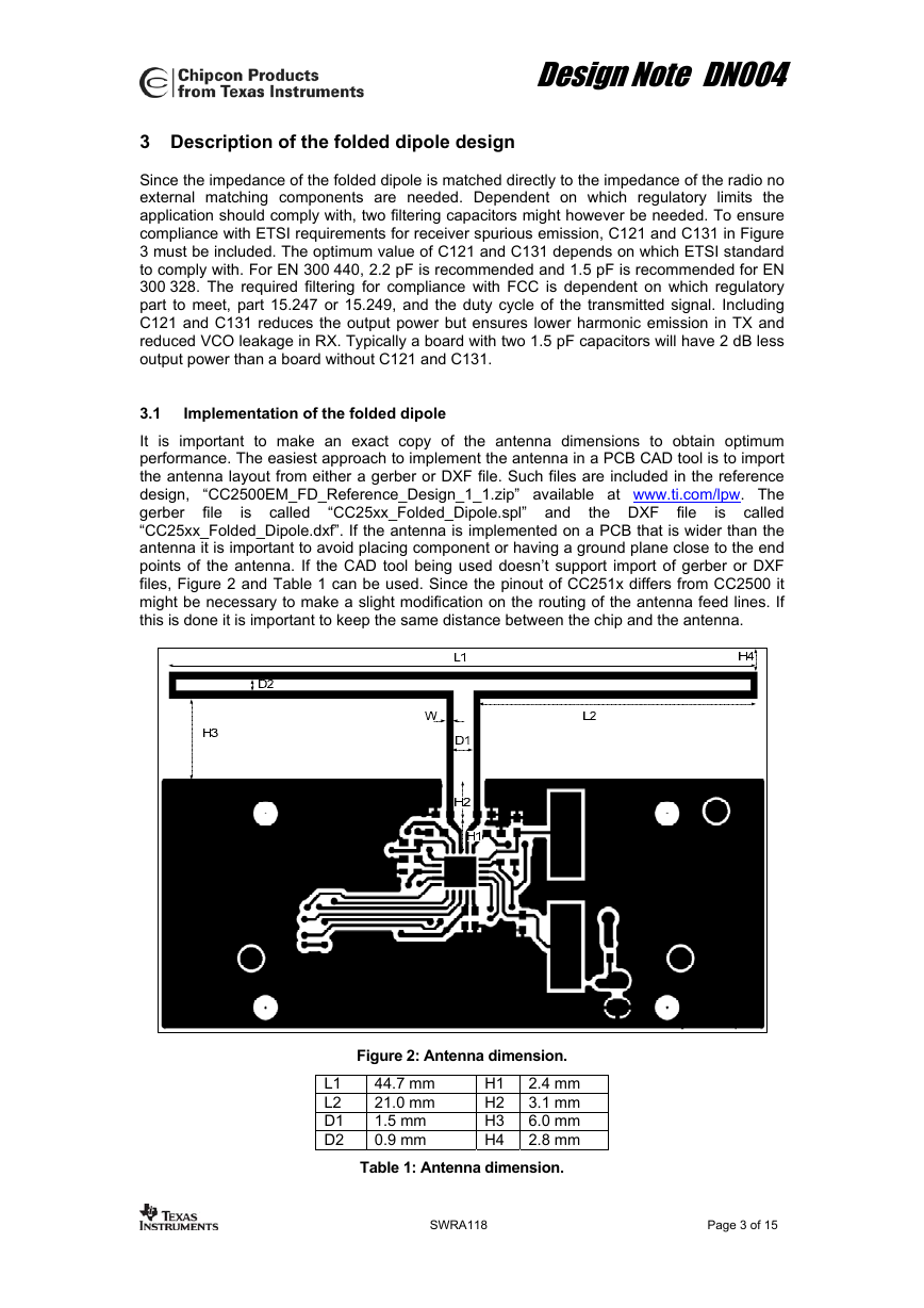
files, Figure 2 and Table 1 can be used. Since the pinout of CC251x differs from CC2500 it
might be necessary to make a slight modification on the routing of the antenna feed lines. If
this is done it is important to keep the same distance between the chip and the antenna.
“CC25xx_Folded_Dipole.spl” and
the DXF
file
Figure 2: Antenna dimension.
L1
L2
D1
D2
44.7 mm
21.0 mm
1.5 mm
0.9 mm
H1
H2
H3
H4
2.4 mm
3.1 mm
6.0 mm
2.8 mm
Table 1: Antenna dimension.
SWRA118
Page 3 of 15
�
Design Note DN004
Figure 3: Schematic for CC2500 folded dipole reference design.
SWRA118
Page 4 of 15
�
Design Note DN004
4 Results
All results presented in this chapter are based on measurements performed with the CC2500
Folded Dipole EM placed on SmartRF04EB.
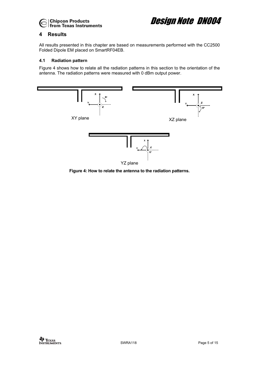
4.1 Radiation pattern
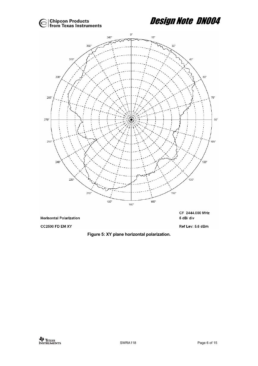
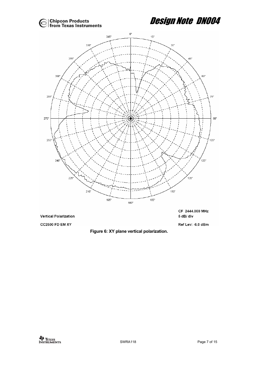
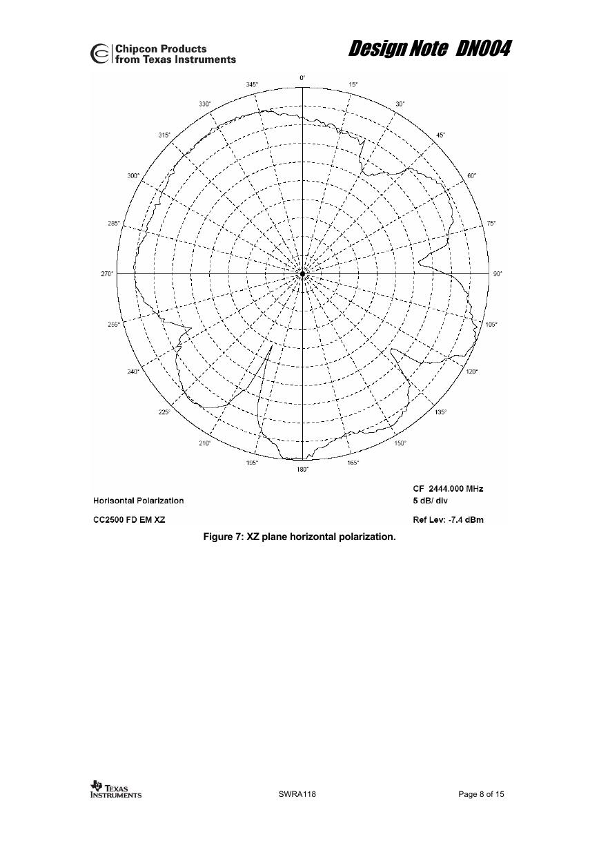
Figure 4 shows how to relate all the radiation patterns in this section to the orientation of the
antenna. The radiation patterns were measured with 0 dBm output power.
XY plane
XZ plane
YZ plane
Figure 4: How to relate the antenna to the radiation patterns.
SWRA118
Page 5 of 15
�
Design Note DN004
Figure 5: XY plane horizontal polarization.
SWRA118
Page 6 of 15
�
Design Note DN004
Figure 6: XY plane vertical polarization.
SWRA118
Page 7 of 15
�
Design Note DN004
Figure 7: XZ plane horizontal polarization.
SWRA118
Page 8 of 15
�
