Document Number: MMA7260QT
Rev 5, 03/2008
MMA7260QT
MMA7260QT: XYZ AXIS
ACCELEROMETER
±1.5g/2g/4g/6g
Bottom View
16 LEAD
QFN
CASE 1622-02
Top View
C
N
/
16
T
U
O
X
T
U
O
Y
T
U
O
Z
15
14
13
g-Select1
g-Select2
VDD
VSS
1
2
3
4
Sleep
Mode
N/C
N/C
N/C
12
11
10
9
5
6
7
8
C
N
/
C
N
/
C
N
/
C
N
/
Figure 1. Pin Connections
Freescale Semiconductor
Technical Data
±1.5g - 6g Three Axis Low-g
Micromachined Accelerometer
The MMA7260QT low cost capacitive micromachined accelerometer
features signal conditioning, a 1-pole low pass filter, temperature
compensation and g-Select which allows for the selection among 4
sensitivities. Zero-g offset full scale span and filter cut-off are factory set and
require no external devices. Includes a Sleep Mode that makes it ideal for
handheld battery powered electronics.
Low Current Consumption: 500 μA
Low Voltage Operation: 2.2 V – 3.6 V
6mm x 6mm x 1.45mm QFN
Features
• Selectable Sensitivity (1.5g/2g/4g/6g)
•
• Sleep Mode: 3 μA
•
•
• High Sensitivity (800 mV/g @ 1.5g)
•
•
• Robust Design, High Shocks Survivability
• Pb-Free Terminations
• Environmentally Preferred Package
•
Low Cost
Fast Turn On Time
Integral Signal Conditioning with Low Pass Filter
Laptop PC: Freefall Detection, Anti-Theft
Typical Applications
• HDD MP3 Player: Freefall Detection
•
• Cell Phone: Image Stability, Text Scroll, Motion Dialing, E-Compass
• Pedometer: Motion Sensing
• PDA: Text Scroll
• Navigation and Dead Reckoning: E-Compass Tilt Compensation
• Gaming: Tilt and Motion Sensing, Event Recorder
• Robotics: Motion Sensing
ORDERING INFORMATION
Device Name
Temperature
Range
MMA7260QT
–40 to +105°C
MMA7260QR2
–40 to +105°C
Package
Drawing
1622-02
1622-02
Package
QFN-16, Tray
QFN-16,Tape & Reel
© Freescale Semiconductor, Inc., 2005-2008. All rights reserved.
�
VDD
g-Select1
g-Select2
Oscillator
Clock
Generator
X-Temp
Comp
Sleep Mode
G-Cell
Sensor
C to V
Converter
Gain
+
Filter
Control Logic
EEPROM Trim Circuits
VSS
Y-Temp
Comp
Z-Temp
Comp
Figure 2. Simplified Accelerometer Functional Block Diagram
XOUT
YOUT
ZOUT
Table 1. Maximum Ratings
(Maximum ratings are the limits to which the device can be exposed without causing permanent damage.)
Rating
Maximum Acceleration (all axis)
Supply Voltage
Drop Test(1)
Storage Temperature Range
1. Dropped onto concrete surface from any axis.
Symbol
gmax
VDD
Ddrop
Tstg
Value
±5000
–0.3 to +3.6
1.8
–40 to +125
Unit
g
V
m
°C
ELECTRO STATIC DISCHARGE (ESD)
WARNING: This device is sensitive to electrostatic
discharge.
Although the Freescale accelerometer contains internal
2000 volts ESD protection circuitry, extra precaution must be
taken by the user to protect the chip from ESD. A charge of
over 2000 volts can accumulate on the human body or
associated test equipment. A charge of this magnitude can
alter the performance or cause failure of the chip. When
handling the accelerometer, proper ESD precautions should
be followed to avoid exposing the device to discharges which
may be detrimental to its performance.
MMA7260QT
2
Sensors
Freescale Semiconductor
�
Table 2. Operating Characteristics
Unless otherwise noted: –40°C < TA < 105°C, 2.2 V < VDD < 3.6 V, Acceleration = 0g, Loaded output(1)
Characteristic
Symbol
Operating Range(2)
Supply Voltage(3)
Supply Current
Supply Current at Sleep Mode(4)
Operating Temperature Range
Acceleration Range, X-Axis, Y-Axis, Z-Axis
g-Select1 & 2: 00
g-Select1 & 2: 10
g-Select1 & 2: 01
g-Select1 & 2: 11
Output Signal
Zero-g (TA = 25°C, VDD = 3.3 V)(5)
Zero-g(4)
X-axis
Y-axis
Z-axis
Sensitivity (TA = 25°C, VDD = 3.3 V)
1.5g
2g
4g
6g
X-axis
Y-axis
Z-axis
Sensitivity(4)
XY
Z
Noise
Bandwidth Response
RMS (0.1 Hz – 1 kHz)(4)
Power Spectral Density RMS (0.1 Hz – 1 kHz)(4)
Control Timing
Power-Up Response Time(8)
Enable Response Time(9)
Sensing Element Resonant Frequency
XY
Z
Internal Sampling Frequency
Output Stage Performance
Full-Scale Output Range (IOUT = 30 µA)
Min
2.2
—
—
–40
—
—
—
—
1.485
±2.6(6)
±5.8(6)
±1.0(6)
740
555
277.5
185
±0.02(6)
±0.01(6)
±0.01(6)
—
—
—
—
—
—
—
—
—
VSS+0.25
Typ
3.3
500
3.0
—
±1.5
±2.0
±4.0
±6.0
1.65
±0.6
±5.8
±0.8
800
600
300
200
±0.02
±0.01
±0.00
350
150
4.7
350
1.0
0.5
6.0
3.4
11
—
Max
3.6
800
10
+105
—
—
—
—
1.815
±3.8(7)
±5.9(7)
±0.8(7)
860
645
322.5
215
±0.02(7)
±0.01(7)
±0.01(7)
—
—
—
—
2.0
2.0
—
—
—
VDD–0.25
Unit
V
μA
μA
°C
g
g
g
g
V
mg/°C
mV/g
mV/g
mV/g
mV/g
%/°C
Hz
Hz
mVrms
μg/
Hz
ms
ms
kHz
kHz
kHz
V
VDD
IDD
IDD
TA
gFS
gFS
gFS
gFS
VOFF
VOFF, TA
S1.5g
S2g
S4g
S6g
S,TA
f-3dB
f-3dB
nRMS
nPSD
tRESPONSE
tENABLE
fGCELL
fGCELL
fCLK
VFSO
NLOUT
Nonlinearity, XOUT, YOUT, ZOUT
Cross-Axis Sensitivity(10)
Ratiometric Error(11)
1. For a loaded output, the measurements are observed after an RC filter consisting of a 1.0 kΩ resistor and a 0.1 µF capacitor on VDD-GND.
2. These limits define the range of operation for which the part will meet specification.
3. Within the supply range of 2.2 and 3.6 V, the device operates as a fully calibrated linear accelerometer. Beyond these supply limits the device
+1.0
5.0
—
–1.0
—
—
—
—
—
VXY, XZ, YZ
error
%FSO
%
%
may operate as a linear device but is not guaranteed to be in calibration.
4. This value is measured with g-Select in 1.5g mode.
5. The device can measure both + and – acceleration. With no input acceleration the output is at midsupply. For positive acceleration the output
will increase above VDD/2. For negative acceleration, the output will decrease below VDD/2.
6. These values represent the 10th percentile, not the minimum.
7. These values represent the 90th percentile, not the maximum.
8. The response time between 10% of full scale VDD input voltage and 90% of the final operating output voltage.
9. The response time between 10% of full scale Sleep Mode input voltage and 90% of the final operating output voltage.
10. A measure of the device’s ability to reject an acceleration applied 90 from the true axis of sensitivity.
11. Zero-g offset ratiometric error can be typically >20% at VDD = 2.2 V. Sensitivity ratiometric error can be typically >3% at VDD = 2.2. Consult
factory for additional information
Sensors
Freescale Semiconductor
MMA7260QT
3
�
PRINCIPLE OF OPERATION
The Freescale accelerometer is a surface-micromachined
integrated-circuit accelerometer.
The device consists of two surface micromachined
capacitive sensing cells (g-cell) and a signal conditioning
ASIC contained in a single integrated circuit package. The
sensing elements are sealed hermetically at the wafer level
using a bulk micromachined cap wafer.
The g-cell is a mechanical structure formed from
semiconductor materials (polysilicon) using semiconductor
processes (masking and etching). It can be modeled as a set
of beams attached to a movable central mass that move
between fixed beams. The movable beams can be deflected
from their rest position by subjecting the system to an
acceleration (Figure 3).
As the beams attached to the central mass move, the
distance from them to the fixed beams on one side will
increase by the same amount that the distance to the fixed
beams on the other side decreases. The change in distance
is a measure of acceleration.
The g-cell beams form two back-to-back capacitors
(Figure 3). As the center beam moves with acceleration, the
distance between the beams changes and each capacitor's
value will change, (C = Aε/D). Where A is the area of the
beam, ε is the dielectric constant, and D is the distance
between the beams.
The ASIC uses switched capacitor techniques to measure
the g-cell capacitors and extract the acceleration data from
the difference between the two capacitors. The ASIC also
signal conditions and filters (switched capacitor) the signal,
providing a high level output voltage that is ratiometric and
proportional to acceleration.
Acceleration
SPECIAL FEATURES
g-Select
The g-Select feature allows for the selection among 4
sensitivities present in the device. Depending on the logic
input placed on pins 1 and 2, the device internal gain will be
changed allowing it to function with a 1.5g, 2g, 4g, or 6g
sensitivity (Table 3). This feature is ideal when a product has
applications requiring different sensitivities for optimum
performance. The sensitivity can be changed at anytime
during the operation of the product. The g-Select1 and
g-Select2 pins can be left unconnected for applications
requiring only a 1.5g sensitivity as the device has an internal
pull-down to keep it at that sensitivity (800mV/g).
Table 3. g-Select Pin Descriptions
g-Select2
g-Select1
g-Range
0
0
1
1
0
1
0
1
1.5g
2g
4g
6g
Sensitivity
800 mV/g
600 mV/g
300 mV/g
200 mV/g
Sleep Mode
The 3 axis accelerometer provides a Sleep Mode that is
ideal for battery operated products. When Sleep Mode is
active, the device outputs are turned off, providing significant
reduction of operating current. A low input signal on pin 12
(Sleep Mode) will place the device in this mode and reduce
the current to 3 μA typ. For lower power consumption, it is
recommended to set g-Select1 and g-Select2 to 1.5g mode.
By placing a high input signal on pin 12, the device will
resume to normal mode of operation.
Filtering
The 3 axis accelerometer contains onboard single-pole
switched capacitor filters. Because the filter is realized using
switched capacitor techniques, there is no requirement for
external passive components (resistors and capacitors) to set
the cut-off frequency.
Figure 3. Simplified Transducer Physical Model
Ratiometricity
Ratiometricity simply means the output offset voltage and
sensitivity will scale linearly with applied supply voltage. That
is, as supply voltage is increased, the sensitivity and offset
increase linearly; as supply voltage decreases, offset and
sensitivity decrease linearly. This is a key feature when
interfacing to a microcontroller or an A/D converter because
it provides system level cancellation of supply induced errors
in the analog to digital conversion process. Offset ratiometric
error can be typically >20% at VDD = 2.2 V. Sensitivity
ratiometric error can be typically >3% at VDD = 2.2 V. Consult
factory for additional information.
MMA7260QT
4
Sensors
Freescale Semiconductor
�
BASIC CONNECTIONS
PCB Layout
Pin Descriptions
Top View
C
N
/
16
T
U
O
X
T
U
O
Y
T
U
O
Z
15
14
13
g-Select1
g-Select2
VDD
VSS
1
2
3
4
12
11
10
9
Sleep Mode
N/C
N/C
N/C
5
6
7
8
/
C
N
/
C
N
/
C
N
/
C
N
Figure 4. Pinout Description
POWER SUPPLY
VDD
VSS
Sleep Mode
g-Select1
g-Select2
XOUT
YOUT
ZOUT
r
e
t
e
m
o
r
e
e
c
c
A
l
C
C
C
R
R
R
C
C
C
VRH
P0
P1
P2
A/DIN
A/DIN
A/DIN
r
e
l
l
o
r
t
n
o
c
o
r
c
M
i
VDD
VSS
C
C
Figure 6. Recommended PCB Layout for Interfacing
Accelerometer to Microcontroller
NOTES:
1. Verify VDD line has the ability to reach 2.2 V in < 0.1
ms as measured on the device at the VDD pin. Rise
times greater than this most likely will prevent start up
operation.
2. Physical coupling distance of the accelerometer to
the microcontroller should be minimal.
3. The flag underneath the package is internally
connected to ground. It is not recommended for the
flag to be soldered down.
4. Place a ground plane beneath the accelerometer to
reduce noise, the ground plane should be attached to
all of the open ended terminals shown in Figure 6.
5. Use an RC filter with 1.0 kΩ and 0.1 µF on the
outputs of the accelerometer to minimize clock noise
(from the switched capacitor filter circuit).
6. PCB layout of power and ground should not couple
power supply noise.
7. Accelerometer and microcontroller should not be a
high current path.
8. A/D sampling rate and any external power supply
switching frequency should be selected such that
they do not interfere with the internal accelerometer
sampling frequency (11 kHz for the sampling
frequency). This will prevent aliasing errors.
9. PCB layout should not run traces or vias under the
QFN part. This could lead to ground shorting to the
accelerometer flag.
Table 4. Pin Descriptions
Pin No.
1
2
3
4
5 - 7
8 - 11
12
13
14
15
16
Pin Name
g-Select1
g-Select2
VDD
VSS
N/C
N/C
Sleep Mode
ZOUT
YOUT
XOUT
N/C
Logic
Inputs
Description
Logic input pin to select g level.
Logic input pin to select g level.
Power Supply Input
Power Supply Ground
No internal connection.
Leave unconnected.
Unused for factory trim.
Leave unconnected.
Logic input pin to enable product or
Sleep Mode.
Z direction output voltage.
Y direction output voltage.
X direction output voltage.
No internal connection.
Leave unconnected.
1
g-Select1
ZOUT
13
1 kΩ
VDD
2
g-Select2
MMA7260QT
3
4
12
VDD
VSS
Sleep Mode
0.1 μF
Logic
Input
0.1 μF
14
1 kΩ
0.1 μF
YOUT
15
1 kΩ
XOUT
0.1 μF
Figure 5. Accelerometer with Recommended
Connection Diagram
Sensors
Freescale Semiconductor
MMA7260QT
5
�
+X
1
2
3
4
Top View
+Y
16
15
14
13
5
6
7
8
-Y
16-Pin QFN Package
12
11
10
9
DYNAMIC ACCELERATION
Side View
-X
-X
-Z
p
o
T
m
o
t
t
o
B
+Z
: Arrow indicates direction of mass movement.
STATIC ACCELERATION
Top View
Direction of Earth’s gravity field.*
XOUT@ 0g = 1.65 V
YOUT @ -1g = 0.85 V
ZOUT@ 0g = 1.65 V
XOUT @ +1g = 2.45 V
YOUT @ 0g = 1.65 V
ZOUT@ 0g = 1.65 V
XOUT @ -1g = 0.85 V
YOUT @ 0g = 1.65 V
ZOUT@ 0g = 1.65 V
Side View
XOUT @ 0g = 1.65 V
YOUT @ 0g = 1.65 V
ZOUT@ +1g = 2.45 V
XOUT @ 0g = 1.65 V
YOUT @ 0g = 1.65 V
ZOUT@ -1g = 0.85 V
XOUT @ 0g = 1.65 V
YOUT @ +1g = 2.45 V
ZOUT@ 0g = 1.65 V
* When positioned as shown, the Earth’s gravity will result in a positive 1g output.
MMA7260QT
6
Sensors
Freescale Semiconductor
�
MINIMUM RECOMMENDED FOOTPRINT FOR SURFACE MOUNTED APPLICATIONS
Surface mount board layout is a critical portion of the total
design. The footprint for the surface mount packages must be
the correct size to ensure proper solder connection interface
between the board and the package.
With the correct footprint, the packages will self-align when
ground. It is not recommended for the flag to be soldered
down.
subjected to a solder reflow process. It is always
recommended to design boards with a solder mask layer to
avoid bridging and shorting between solder pads.
The flag underneath the package is internally connected to
Pin 1 ID
(non-metallic)
Do not solder down
flag and 4 corner
ground pads on the
package for
consumer application
Do not place any top
metal patterns or via
structures beneath
the package
Note: The die pad (flag) is not generally recommended to be
soldered down for consumer product application. All dimensions
are in mm.
Figure 7. PCB Footprint for 16-Lead QFN, 6x6 mm for
Consumer Grade Products and Applications
Sensors
Freescale Semiconductor
MMA7260QT
7
�
PCB DESIGN GUIDELINES
The following are the recommended guidelines to follow
for mounting QFN sensors for either automotive or consumer
applications.
1. NSMD (Non Solder Mask Defined) is shown in
Figure 8.
2. Solder mask opening = PCB land pad +0.1 mm.
3. Stencil aperture size = PCB land pad –0.025mm, as
shown in Figure 9 with a 6mil stencil.
4. Do not place insertion components or vias at a
distance less than 2mm from the package land area.
5. Signal trace connected to pads should be as
symmetric as possible. Put dummy traces if there is
NC pads, in order to have same length of exposed
trace for all pads. Signal traces with 0.1mm width and
min. 0.5mm length for all PCB land pad near package
are recommended as shown in Figure 8 and
Figure 9. Wider trace can be continued after the
0.5mm zone.
6. Use a standard pick and place process and
equipment (no hand soldering process).
7. It is recommended to use a cleanable solder paste
with an additional cleaning step after SMT mount
8. It is recommended to avoid screwing down the PCB
to fix it into an enclosure since this may cause the
PCB to bend.
9. PC boards should be rated for multiple reflow of lead-
free conditions with 260°C maximum temperature.
Package Pad
PCB land pattern - NSMD
Signal trace 0.1mm width
and 0.5mm (min) length near
package. Wider trace can be
continued after these traces.
0.50 mm
0.55 mm
Cu: 0.55 x 0.50 mm sq.
Solder mask opening =
PCB land pad +0.1mm
=0.65x0.60 mm sq.
Figure 8. NSMD Solder Mask Design Guidelines
Signal trace near package: 0.1mm width and
0.5mm (min) length are recommended near
package. Wider trace can be continued after
these.
Stencil opening (black) for land pad (yellow)
= PCB landing pad -0.025mm
= 0.525mmx0,475mm
Package foot pirnt
Figure 9. Stencil Design Guidelines
MMA7260QT
8
Sensors
Freescale Semiconductor
�

.pdf-第1页.png")
.pdf-第2页.png")
.pdf-第3页.png")
.pdf-第4页.png")
.pdf-第5页.png")
.pdf-第6页.png")
.pdf-第7页.png")
.pdf-第8页.png")
 Meta大模型论文:The Llama 3 Herd of Models.pdf
 ACS0709(传感器资料).PDF
 495个C语言常见问题集.pdf
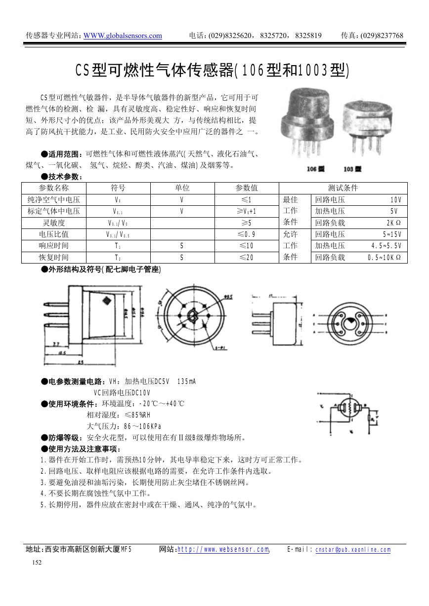 CS型可燃性气体传感器(106型和1003型)(传感器资料).pdf
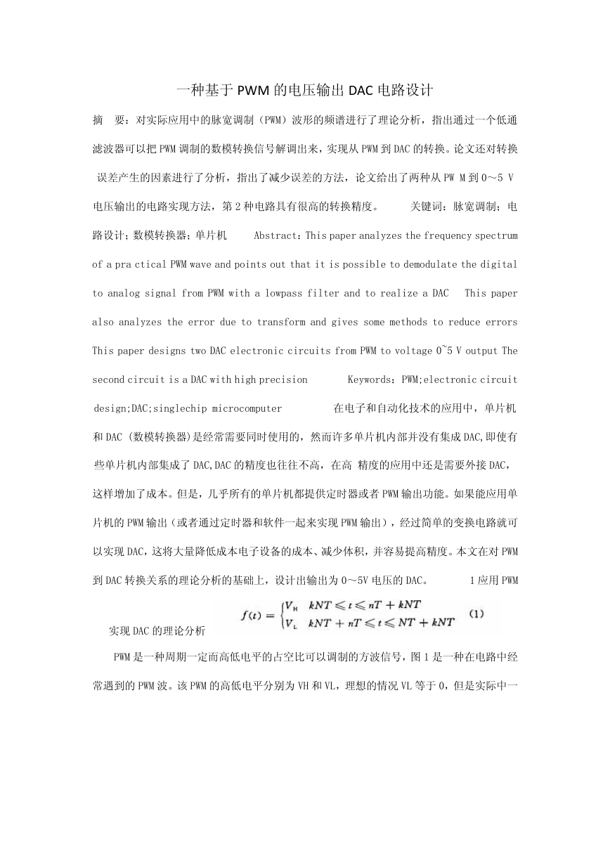 一种基于PWM的电压输出DAC电路设计.pdf
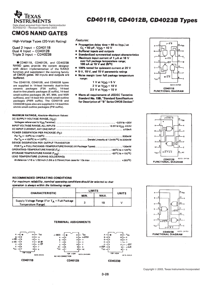 cd4011b(智能车电机驱动).pdf
 电路设计规范_中兴.pdf
 HA50-P(传感器资料).pdf
 ETD-core(TDK磁芯资料).pdf