查询TDA1311A供应商
DATA SHEETPreliminary specificationSupersedes data of July 1993File under Integrated Circuits, IC011995Dec18INTEGRATED CIRCUITSTDA1311AStereo Continuous Calibration DAC(CC-DAC)�
1995Dec182Philips SemiconductorsPreliminary specificationStereo Continuous Calibration DAC(CC-DAC)TDA1311AFEATURES•Voltage output•Space saving packages SO8 or DIP8•Low power consumption•Wide dynamic range (16-bit resolution)•Continuous Calibration (CC) concept•Easy application:–single 4to5.5V rail supply–output current and bias current are proportional to thesupply voltage–integrated current-to-voltage converter•Fast settling time permits 2, 4 and8·oversampling(serial input) or double-speed operation at4·oversampling•Internal bias current ensures maximum dynamic range•Wide operating temperature range (-40Cto+85C)•Compatible with most current Japanese input formats:time multiplexed, two's complement, TTL•No zero-crossing distortion•Cost efficient.GENERAL DESCRIPTIONThe TDA1311A; AT is a voltage-driven digital-to-analogconverter and is new generation of DAC devices whichembodies the innovative technique of ContinuousCalibration (CC). The largest bit-currents are repeatedlygenerated by one single current reference source. Thisduplication is based upon an internal charge storageprinciple which has an accuracy insensitive to ageing,temperature matching and process variations.The TDA1311A; AT is fabricated in a 1.0mm CMOSprocess and features an extremely low-power dissipation,small package size and easy application. Furthermore, theaccuracy of the intrinsic high coarse-current combinedwith the implemented symmetrical offset decoding methodpreclude zero-crossing distortion and ensures high qualityaudio reproduction. Therefore, the CC-DAC is eminentlysuitable for use in (portable) digital audio equipment.ORDERING INFORMATIONTYPENUMBERPACKAGENAMEDESCRIPTIONVERSIONTDA1311ADIP8plastic dual in-line package; 8leads (300mil)SOT97-1TDA1311ATSO8plastic small outline package; 8leads; body width 3.9mmSOT96-1�
1995Dec183Philips SemiconductorsPreliminary specificationStereo Continuous Calibration DAC(CC-DAC)TDA1311AQUICK REFERENCE DATASYMBOLPARAMETERCONDITIONSMIN.TYP.MAX.UNITVDDsupply voltage455.5VIDDsupply currentVDD=5V at code 0000H-3.46.0mAVFSfull scale output voltageVDD=5V1.82.02.2V(THD+N)/Stotal harmonic distortionplus noiseat 0dB signal level--68-63dB-0.040.07%at-60dB signal level--30-24dB-36%at-60dB signal level;A-weighted--33-dB-2-%S/Nsignal-to-noise ratio atbipolar zeroA-weighted at code 0000H8692-dBtcscurrent settling time to–1LSB-0.2-msBRinput bit rate at data input--18.4Mbits/sfBCKclock frequency at clockinput--18.4MHzTCFSfull scale temperaturecoefficient at analog outputs(IOL; IOR)-–400-ppmTamboperating ambienttemperature-40-+85CPtottotal power dissipationVDD=5V at code 0000H-1730mW�
1995Dec184Philips SemiconductorsPreliminary specificationStereo Continuous Calibration DAC(CC-DAC)TDA1311ABLOCK DIAGRAMFig.1 Block diagram.handbook, full pagewidthMBG85832 (5-BIT)CALIBRATEDCURRENTSOURCES1 CALIBRATEDSPARE SOURCE11-BITPASSIVEDIVIDERLEFT BIT SWITCHES6I/VLEFT INPUT REGISTERLEFT OUTPUT REGISTERRIGHT BIT SWITCHESRIGHT INPUT REGISTERRIGHT OUTPUT REGISTER8I/V32 (5-BIT)CALIBRATEDCURRENTSOURCES1 CALIBRATEDSPARE SOURCE11-BITPASSIVEDIVIDERREFERENCE SOURCECONTROLAND TIMING12354C2100 nFVDDVORIORGNDTDA1311ATDA1311ATVOLBCKWSDATAIOLPINNINGSYMBOLPINDESCRIPTIONBCK1bit clock inputWS2word select inputDATA3data inputGND4groundVDD5supply voltageVOL6left channel outputn.c.7not connectedVOR8right channel outputFig.2 Pin configuration.handbook, halfpage12348765MBG859TDA1311ATDA1311ATBCKWSDATAGNDVDDVOLVORn.c.�
1995Dec185Philips SemiconductorsPreliminary specificationStereo Continuous Calibration DAC(CC-DAC)TDA1311AFUNCTIONAL DESCRIPTIONThe basic operation of the continuous calibration DAC isillustrated inFig.3. The figure shows the calibration andoperation cycle. During calibration of the MOS currentsource (seeFig.3a) transistor M1 is connected as a diodeby applying a reference current. The voltage Vgs on theintrinsic gate-source capacitance Cgs of M1 is thendetermined by the transistor characteristics. Aftercalibration of the drain current to the reference value IREF,the switch S1 is opened and S2 is switched to the otherposition (see Fig.3b). The gate-to-source voltage Vgs ofM1 is not changed because the charge on Cgs ispreserved. Therefore, the drain current of M1 will still beequal to IREF and this exact duplicate of IREF is nowavailable at the OUT terminal.The 32current sources and the spare current source of theTDA1311A; AT are continuously calibrated(see Fig.1).The spare current source is included to allow continuousconverter operation. The output of one calibrated source isconnected to an 11-bit binary current divider consisting of2048transistors.A symmetrical offset decoding principle is incorporatedthat arranges the bit switching in such a way that thezero-crossing is performed only by switching the LSBcurrents.The TDA1311A; AT (CC-DAC) accepts serial input dataformats of 16-bit word length. Left and right data words aretime multiplexed. The most significant bit (bit1) mustalways be first. The input data format is shown in Figs4and 5.With a HIGH level on the word select input (WS), data isplaced in the left input register and with a LOW level on theWS input, data is placed in the right input register (seeFig.1). The data in the input registers are simultaneouslylatched in the output registers which control the bitswitches.An internal offset voltage VOS is added to the full scaleoutput voltage VFS; VOS and VFS are proportional to VDD:VDD1/VDD2=VFS1/VFS2=VOS1/VOS2.Fig.3 Calibration principle.handbook, full pagewidthMBG860outS2S1M1CgsVgsCgsVgsoutS2S1M1IrefIrefIref(a)(b)(a)=calibration.(b)=operation.�
1995Dec186Philips SemiconductorsPreliminary specificationStereo Continuous Calibration DAC(CC-DAC)TDA1311ALIMITING VALUESIn accordance with the Absolute Maximum Rating System (IEC134).Note1.Human body model: C=100pF, R=1500W, 3pulses positive and 3pulses negative.2.Machine model: C=200pF, L=0.5mH, R=10W, 3pulses positive and 3pulses negative.THERMAL RESISTANCEQUALITY SPECIFICATIONIn accordance with SNW-FQ-0611.CHARACTERISTICSVDD=5V; Tamb=25C; measured in Fig.1; unless otherwise specified.SYMBOLPARAMETERCONDITIONSMIN.MAX.UNITVDDsupply voltage-6.0VTstgstorage temperature-55+150CTXTALmaximum crystal temperature-+150CTamboperating ambient temperature-40+85CVeselectrostatic handlingnote1-2000+2000Vnote2-200+200VSYMBOLPARAMETERVALUEUNITRth j-athermal resistance from junction to ambient in free airDIL8100K/WSO8210K/WSYMBOLPARAMETERCONDITIONSMIN.TYP.MAX.UNITSupplyVDDsupply voltage4.05.05.5VIDDsupply currentat code 0000H-3.46.0mADigital inputs; pins WS, BCK and DATA|IIL|input leakage current LOWVI=0.8V--10mA|IIH|input leakage current HIGHVI=2.4V--10mAfBCKclock frequency--18.4MHzBRbit rate data input--18.4Mbits/sfWSword select input frequency--384kHz�
1995Dec187Philips SemiconductorsPreliminary specificationStereo Continuous Calibration DAC(CC-DAC)TDA1311ANote1.Measured with 1kHz sinewave generated at sampling rate of 192kHz.Timing(see Fig.4)trrise time--12nstffall time--12nstCYbit clock cycle time54--nstBCKHbit clock pulse width HIGH15--nstBCKLbit clock pulse width LOW15--nstSU;DATdata set-up time12--nstHD:DATdata hold time to bit clock2--nstHD:WSword select hold time2--nstSU;WSword select set-up time12--nsAnalog outputs; pins VOL and VORVFSfull-scale voltage1.82.02.2VTCFSfull-scale temperaturecoefficient-–400-ppmVosoffset voltageVDD=VOL/ORmax0.450.500.55V(THD+N)/Stotal harmonic distortion plusnoiseat 0dB signal level; note1--68-63dB-0.040.07%at-60dB signal level; note1--30-24dB-36%at-60dB signal level;A-weighted; note1--33-dB-2-%at 0dB signal level; f=20Hzto 20kHz--65-61dB-0.050.09%tcscurrent settling time to–1 LSB-0.2-msacschannel separation7580-dB|dIO|unbalance between outputsnote1-0.20.3dB|td|time delay between outputs-–0.2-msS/Nsignal-to-noise ratio atbipolar zeroA-weighted at code 0000H8692-dBSYMBOLPARAMETERCONDITIONSMIN.TYP.MAX.UNIT�
1995Dec188Philips SemiconductorsPreliminary specificationStereo Continuous Calibration DAC(CC-DAC)TDA1311AFig.4 Timing and input signals.handbook, full pagewidthMBG861sample outWSBCKDATARIGHTLSBMSBLEFTtHD; WStSU; WStSU; DATtHD; DATtBCKLtBCKHtftr>12>15>15tCY>54<12<12>2>12>2�

.pdf-第1页.png")
.pdf-第2页.png")
.pdf-第3页.png")
.pdf-第4页.png")
.pdf-第5页.png")
.pdf-第6页.png")
.pdf-第7页.png")
.pdf-第8页.png")
 Meta大模型论文:The Llama 3 Herd of Models.pdf
 ACS0709(传感器资料).PDF
 495个C语言常见问题集.pdf
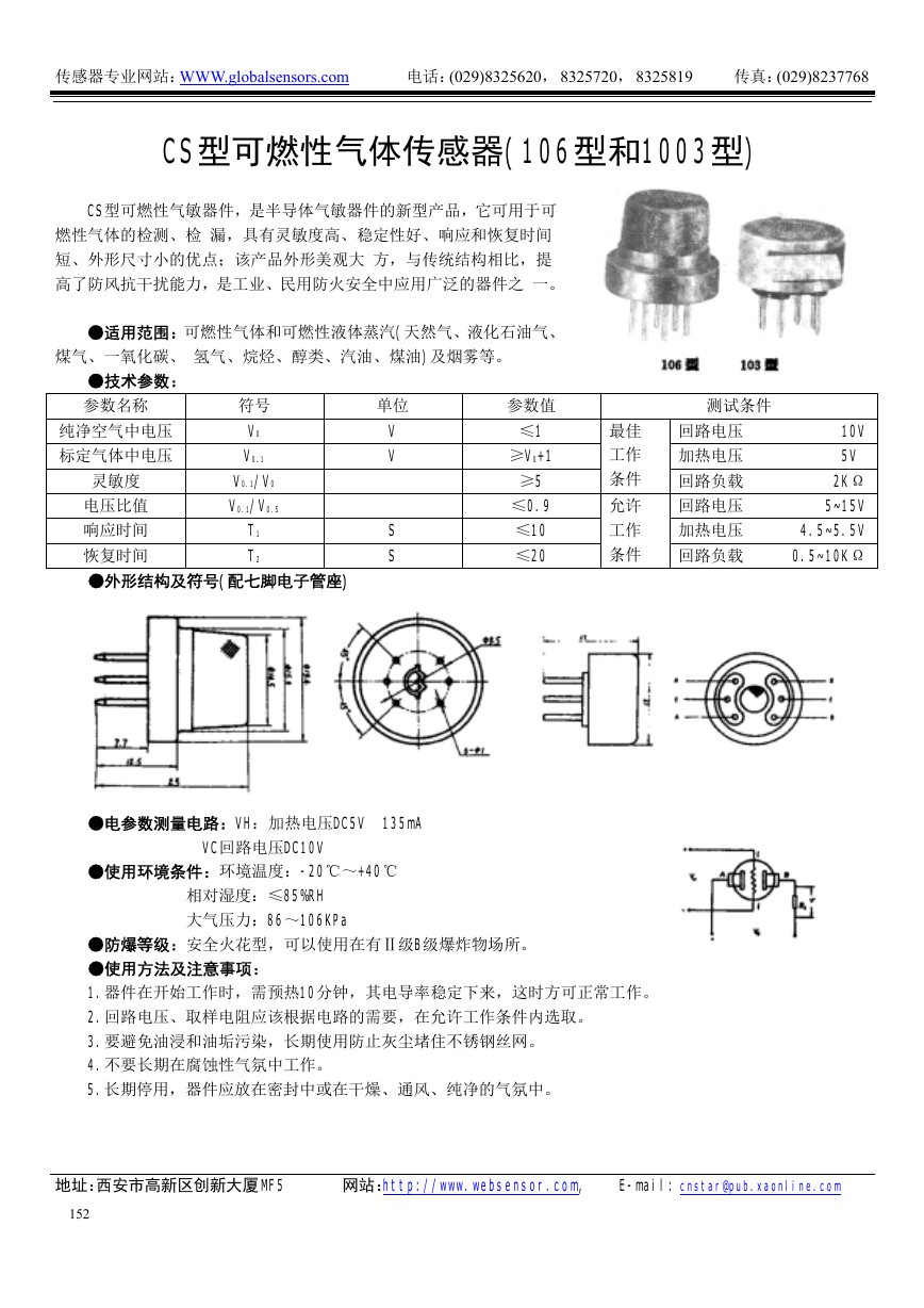 CS型可燃性气体传感器(106型和1003型)(传感器资料).pdf
 一种基于PWM的电压输出DAC电路设计.pdf
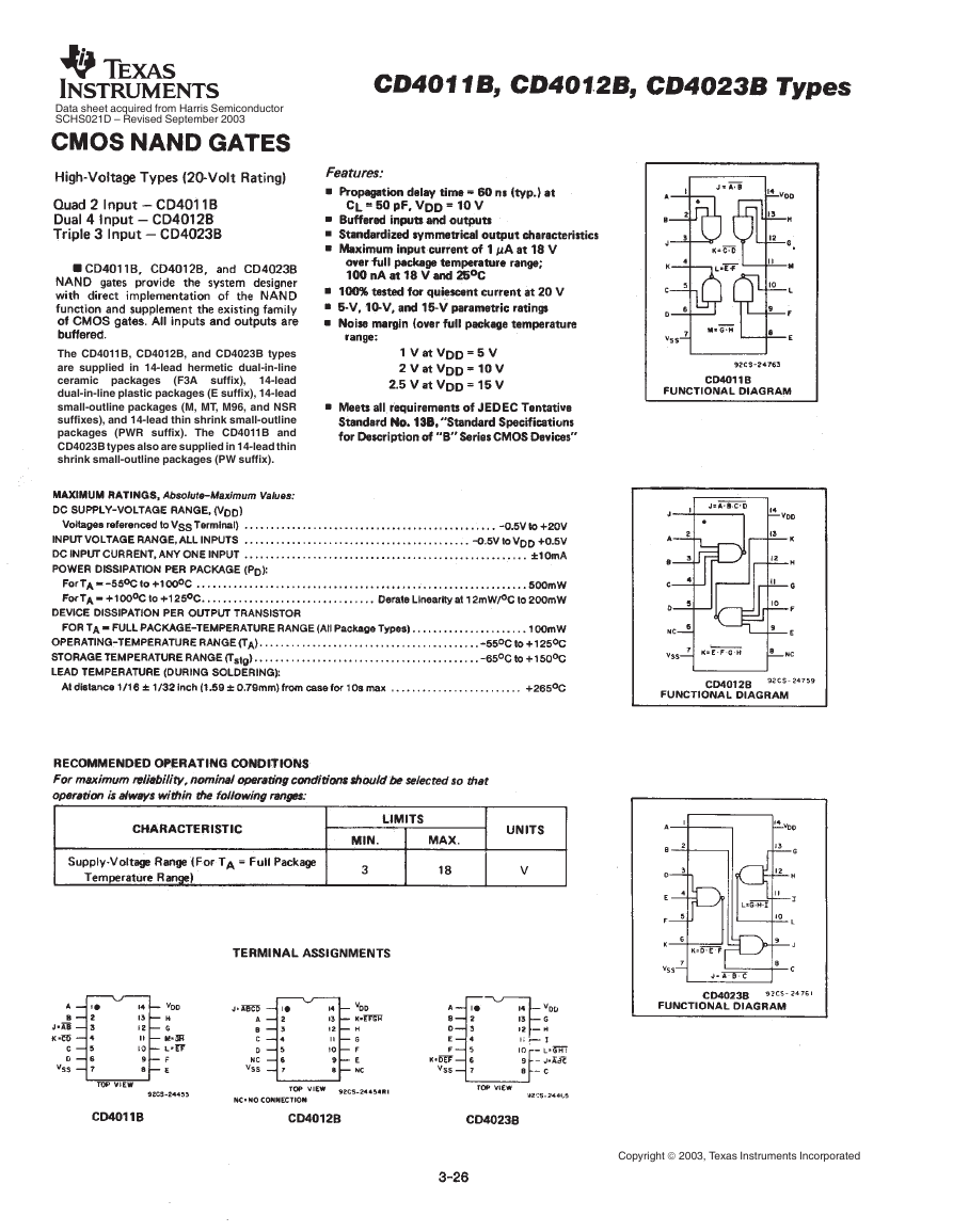 cd4011b(智能车电机驱动).pdf
 电路设计规范_中兴.pdf
 HA50-P(传感器资料).pdf
 ETD-core(TDK磁芯资料).pdf