INTEGRATED CIRCUITS
DATA SHEET
TJA1050
High speed CAN transceiver
Preliminary specification
File under Integrated Circuits, IC18
1999 Sep 27
�
Philips Semiconductors
Preliminary specification
High speed CAN transceiver
TJA1050
FEATURES
• Fully compatible with the “ISO 11898” standard
• High speed (up to 1 Mbaud)
• Transmit Data (TXD) dominant time-out function
• Bus lines protected against transients in an automotive
environment
• Silent mode in which the transmitter is disabled
• Differential receiver with wide common-mode range for
high ElectroMagnetic Immunity (EMI)
• Input levels compatible with 3.3 V devices
• Thermally protected
• Short-circuit proof to battery and ground
• An unpowered node does not disturb the bus lines
• At least 110 nodes can be connected.
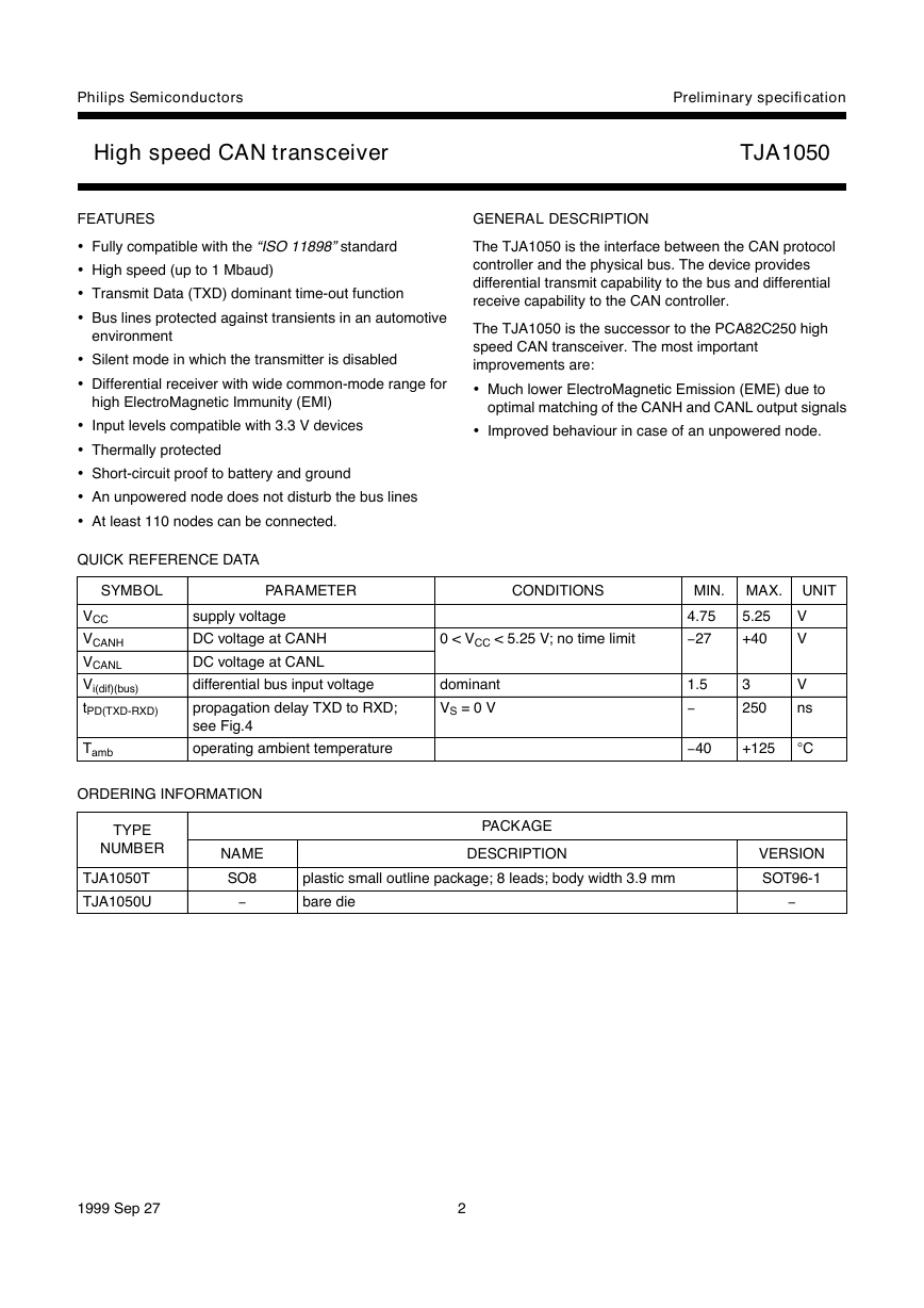
QUICK REFERENCE DATA
GENERAL DESCRIPTION
The TJA1050 is the interface between the CAN protocol
controller and the physical bus. The device provides
differential transmit capability to the bus and differential
receive capability to the CAN controller.
The TJA1050 is the successor to the PCA82C250 high
speed CAN transceiver. The most important
improvements are:
• Much lower ElectroMagnetic Emission (EME) due to
optimal matching of the CANH and CANL output signals
• Improved behaviour in case of an unpowered node.
SYMBOL
VCC
VCANH
VCANL
Vi(dif)(bus)
tPD(TXD-RXD)
Tamb
PARAMETER
CONDITIONS
supply voltage
DC voltage at CANH
DC voltage at CANL
differential bus input voltage
propagation delay TXD to RXD;
see Fig.4
operating ambient temperature
0 < VCC < 5.25 V; no time limit
dominant
VS = 0 V
MIN. MAX. UNIT
4.75
- 27
5.25
+40
V
V
1.5
3
250
- 40
+125
V
ns
C
ORDERING INFORMATION
TYPE
NUMBER
TJA1050T
TJA1050U
NAME
SO8
PACKAGE
DESCRIPTION
plastic small outline package; 8 leads; body width 3.9 mm
bare die
VERSION
SOT96-1
1999 Sep 27
2
-
-
-
�
VCC
3
TEMPERATURE
PROTECTION
DRIVER
Preliminary specification
TJA1050
7
25
kW
25
kW
6
CANH
CANL
Philips Semiconductors
High speed CAN transceiver
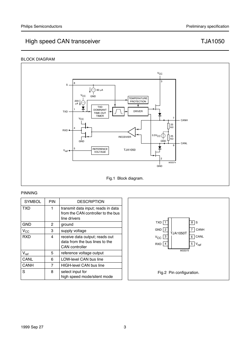
BLOCK DIAGRAM
handbook, full pagewidth
8
S
200
m A
60 m A
VCC
GND
TXD
DOMINANT
TIME-OUT
TIMER
1
4
5
VCC
GND
TXD
RXD
Vref
RECEIVER
0.5VCC
GND
REFERENCE
VOLTAGE
TJA1050
2
GND
MGS374
Fig.1 Block diagram.
PINNING
SYMBOL
TXD
PIN
1
GND
VCC
RXD
Vref
CANL
CANH
S
2
3
4
5
6
7
8
DESCRIPTION
transmit data input; reads in data
from the CAN controller to the bus
line drivers
ground
supply voltage
receive data output; reads out
data from the bus lines to the
CAN controller
reference voltage output
LOW-level CAN bus line
HIGH-level CAN bus line
select input for
high speed mode/silent mode
handbook, halfpage
TXD
GND
VCC
RXD
1
2
3
4
8
S
7
6
5
CANH
CANL
Vref
TJA1050T
MGS375
Fig.2 Pin configuration.
1999 Sep 27
3
�
Preliminary specification
TJA1050
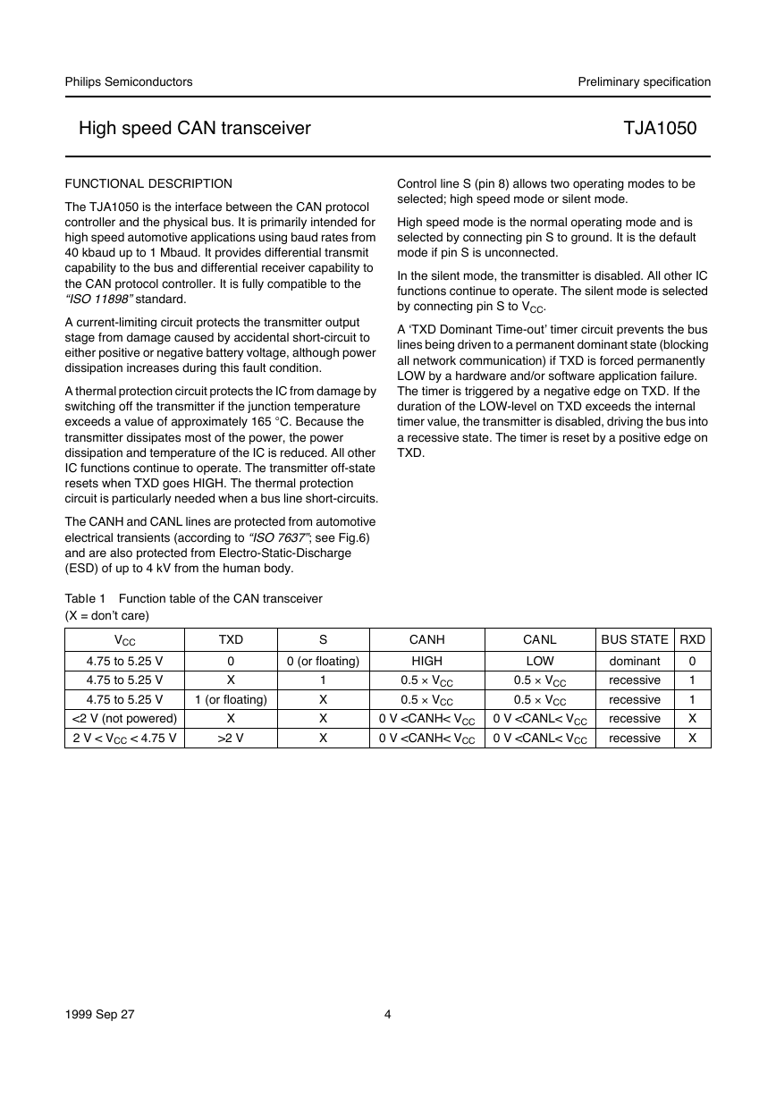
Control line S (pin 8) allows two operating modes to be
selected; high speed mode or silent mode.
High speed mode is the normal operating mode and is
selected by connecting pin S to ground. It is the default
mode if pin S is unconnected.
In the silent mode, the transmitter is disabled. All other IC
functions continue to operate. The silent mode is selected
by connecting pin S to VCC.
A ‘TXD Dominant Time-out’ timer circuit prevents the bus
lines being driven to a permanent dominant state (blocking
all network communication) if TXD is forced permanently
LOW by a hardware and/or software application failure.
The timer is triggered by a negative edge on TXD. If the
duration of the LOW-level on TXD exceeds the internal
timer value, the transmitter is disabled, driving the bus into
a recessive state. The timer is reset by a positive edge on
TXD.
Philips Semiconductors
High speed CAN transceiver
FUNCTIONAL DESCRIPTION
The TJA1050 is the interface between the CAN protocol
controller and the physical bus. It is primarily intended for
high speed automotive applications using baud rates from
40 kbaud up to 1 Mbaud. It provides differential transmit
capability to the bus and differential receiver capability to
the CAN protocol controller. It is fully compatible to the
“ISO11898”standard.
A current-limiting circuit protects the transmitter output
stage from damage caused by accidental short-circuit to
either positive or negative battery voltage, although power
dissipation increases during this fault condition.
A thermal protection circuit protects the IC from damage by
switching off the transmitter if the junction temperature
exceeds a value of approximately 165 C. Because the
transmitter dissipates most of the power, the power
dissipation and temperature of the IC is reduced. All other
IC functions continue to operate. The transmitter off-state
resets when TXD goes HIGH. The thermal protection
circuit is particularly needed when a bus line short-circuits.
The CANH and CANL lines are protected from automotive
electrical transients (according to “ISO 7637”; see Fig.6)
and are also protected from Electro-Static-Discharge
(ESD) of up to 4 kV from the human body.
Table 1 Function table of the CAN transceiver
(X = don’t care)
VCC
4.75 to 5.25 V
4.75 to 5.25 V
4.75 to 5.25 V
TXD
0
X
1 (or floating)
<2 V (not powered)
2 V < VCC < 4.75 V
X
>2 V
S
0 (or floating)
1
X
X
X
CANH
HIGH
0.5 · VCC
0.5 · VCC
CANL
LOW
0.5 · VCC
0.5 · VCC
0 V
Philips Semiconductors
High speed CAN transceiver
Preliminary specification
TJA1050
LIMITING VALUES
In accordance with the Absolute Maximum Rating System (IEC 134). All voltages are referenced to GND (pin 2).
Positive currents flow into the IC.
SYMBOL
VCC
VCANL, VCANH
VTXD, VRXD,
Vref and VS
Vtrt(CANH),
Vtrt(CANL)
Vesd
Tstg
Tamb
Tj
PARAMETER
CONDITIONS
MIN.
MAX.
UNIT
supply voltage
DC voltage at CANL and CANH
DC voltage at TXD, RXD, Vref and S
transient voltage at CANH and CANL
electrostatic discharge at CANH; CANL
electrostatic discharge at TXD; VCC;
RXD; Vref and S
electrostatic discharge at all pins
storage temperature
operating ambient temperature
junction temperature
0 < VCC < 5.25 V;
no time limit
time limit is 1 m s
note 1
note 3
note 3
note 4
note 2
- 0.3
- 27
- 0.3
- 55
- 200
- 4
- 2
- 200
- 55
- 40
- 40
+5.25
+40
V
V
VCC + 0.3 V
+55
+200
+4
+2
+200
+150
+125
+150
V
V
kV
kV
V
C
C
C
Notes
1. The waveforms of the applied transients shall be in accordance with “ISO7637part1”, test pulses 1, 2, 3a and 3b,
2.
(see Fig.6).
In accordance with “IEC747-1”. An alternative definition of Tj is: Tj = Tamb + P · Rth(j-a), where Rth(j-a) is a fixed value
to be used for the calculation of Tj. The rating for Tj limits the allowable combinations of power dissipation (P) and
ambient temperature (Tamb).
3. Human body model; C = 100 pF R = 1.5 kW.
4. Machine model; C = 200 pF R = 25 W
.
THERMAL CHARACTERISTICS
According to IEC 747-1.
SYMBOL
Rth(j-a)
PARAMETER
CONDITIONS
thermal resistance from junction to
ambient; TJA1050T(SO8)
in free air
VALUE
160
UNIT
K/W
QUALITY SPECIFICATION
Quality specification “SNW-FQ-611partD” is applicable.
1999 Sep 27
5
�
Philips Semiconductors
High speed CAN transceiver
Preliminary specification
TJA1050
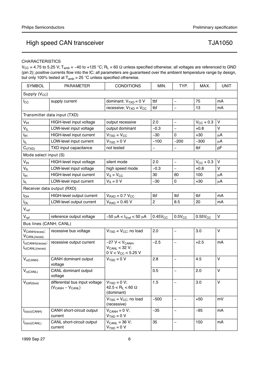
CHARACTERISTICS
VCC = 4.75 to 5.25 V; Tamb = - 40 to +125 C; RL = 60 W unless specified otherwise; all voltages are referenced to GND
(pin 2); positive currents flow into the IC; all parameters are guaranteed over the ambient temperature range by design,
but only 100% tested at Tamb = 25 C unless specified otherwise.
CONDITIONS
PARAMETER
SYMBOL
MIN.
TYP.
MAX.
UNIT
HIGH-level input voltage
LOW-level input voltage
HIGH-level input current
LOW-level input current
TXD input capacitance
HIGH-level input voltage
LOW-level input voltage
HIGH-level input current
LOW-level input current
HIGH-level output current
LOW-level output current
Supply (VCC)
ICC
supply current
Transmitter data input (TXD)
VIH
VIL
IIH
IIL
Ci(TXD)
Mode select input (S)
VIH
VIL
IIH
IIL
Receiver data output (RXD)
IOH
IOL
Vref
Vref
Bus lines (CANH; CANL)
VCANH(reces);
VCANL(reces)
Io(CANH)(reces);
Io(CANL)(reces)
recessive bus voltage
recessive output current
Vo(CANH)
Vo(CANL)
Vi(dif)(bus)
CANH dominant output
voltage
CANL dominant output
voltage
differential bus input voltage
(VCANH - VCANL)
Io(sc)(CANH)
Io(sc)(CANL)
CANH short-circuit output
current
CANL short-circuit output
current
1999 Sep 27
6
reference output voltage
- 50 m A < IVref < 50 m A
0.45VCC
0.5VCC
0.55VCC
dominant; VTXD = 0 V
recessive; VTXD = VCC
tbf
tbf
output recessive
output dominant
VTXD = VCC
VTXD = 0 V
not tested
silent mode
high speed mode
VS = VCC
VS = 0 V
VRXD = 0.7 VCC
VRXD = 0.45 V
2.0
- 0.3
- 30
- 100
2.0
- 0.3
30
- 30
tbf
2
0
- 200
60
0
tbf
8.5
VTXD = VCC; no load
- 27 V < VCANH,
VCANL < 32 V;
0 V < VCC < 5.25 V
VTXD = 0 V
VTXD = 0 V;
42.5 < RL < 60 W
(dominant)
VTXD = VCC; no load
(recessive)
VCANH = 0 V;
VTXD = 0 V
VCANL = 36 V;
VTXD = 0 V
2.0
- 2.5
2.8
0.5
1.5
- 500
- 35
35
75
13
mA
mA
VCC + 0.3 V
V
+0.8
m A
+30
- 300
m A
pF
tbf
VCC + 0.3 V
+0.8
V
m A
100
m A
+30
tbf
20
3.0
mA
mA
V
V
+2.5
mA
4.5
2.0
3.0
+50
- 95
150
V
V
V
mV
mA
mA
-
-
-
-
-
-
-
-
-
-
-
-
-
-
-
-
�
Philips Semiconductors
High speed CAN transceiver
Preliminary specification
TJA1050
SYMBOL
PARAMETER
CONDITIONS
MIN.
TYP.
MAX.
UNIT
V
mV
kW
%
kW
pF
pF
m A
C
ns
ns
differential receiver threshold
voltage
differential receiver input
voltage hysteresis
CANH; CANL common
mode input resistance
matching between CANH
and CANL common mode
input resistance
differential input resistance
CANH; CANL input
capacitance
differential input capacitance
CANH; CANL input leakage
current
- 12 V < VCANH,
VCANL < 12 V; see Fig.5
see Fig.5
0.5
100
10
- 3
20
VCANH = VCANL
VTXD = VCC; not tested
VCC = 0 V;
VCANH = VCANL = 5 V
0.7
25
50
0.9
200
50
+3
100
20
10
500
155
165
180
tbf
tbf
tbf
tbf
150
100
Vdif(th)
Vi(dif)(hys)
Ri(cm)(CANH);
Ri(cm)(CANL)
Ri(cm)(m)
Ri(dif)
Ci(CANH);
Ci(CANL)
Ci(dif)
ILI(CANH);
ILI(CANL)
Thermal shutdown
Tj(sd)
shutdown junction
temperature
Timing characteristics (see Figs 3 and 4)
td(TXD-BUSon)
td(TXD-BUSoff)
td(BUSon-RXD)
td(BUSoff-RXD)
delay TXD to bus active
delay TXD to bus inactive
delay bus active to RXD
delay bus inactive to RXD
VS = 0 V
1999 Sep 27
7
-
-
-
-
-
-
-
-
�
Philips Semiconductors
High speed CAN transceiver
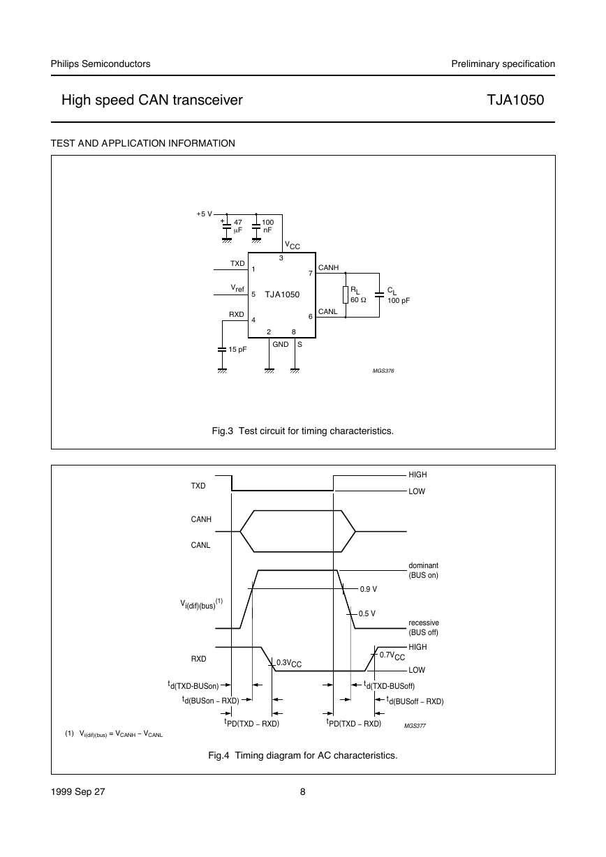
TEST AND APPLICATION INFORMATION
Preliminary specification
TJA1050
+5 V
handbook, halfpage
47
m F
100
nF
VCC
3
TJA1050
2
8
GND S
TXD
Vref
RXD
1
5
4
15 pF
CANH
CANL
7
6
RL
60 W
CL
100 pF
MGS376
Fig.3 Test circuit for timing characteristics.
handbook, full pagewidth
TXD
CANH
CANL
Vi(dif)(bus)
(1)
0.9 V
0.5 V
RXD
0.3VCC
0.7VCC
HIGH
LOW
dominant
(BUS on)
recessive
(BUS off)
HIGH
LOW
(1) Vi(dif)(bus) = VCANH - VCANL
td(TXD-BUSon)
td(BUSon - RXD)
td(TXD-BUSoff)
td(BUSoff - RXD)
tPD(TXD - RXD)
tPD(TXD - RXD)
MGS377
Fig.4 Timing diagram for AC characteristics.
1999 Sep 27
8
�
