19-0550; Rev 1; 2/11
Low-Cost Stereo Audio DAC
M
A
X
5
5
5
6
General Description
The MAX5556 stereo audio sigma-delta digital-to-analog
converter (DAC) offers a simple and complete stereo
digital-to-analog solution for media servers, set-top
boxes, video-game hardware, automotive rear-seat
entertainment, and other general consumer audio appli-
cations. This DAC features built-in digital interpolation/fil-
tering, sigma-delta digital-to-analog conversion, and
analog output filtering. Control logic and mute circuitry
minimize audible pops and clicks during power-up,
power-down, clock changes, or when invalid clock con-
ditions occur.
The MAX5556 receives input data over a 3-wire
I2S-compatible interface with left-justified audio data.
Data can be clocked by either an external or internal
serial clock. The internal serial clock frequency is pro-
grammable by selection of a master clock (MCLK) and
sample clock (LRCLK) ratio. Sampling rates from 2kHz
to 50kHz are supported.
The MAX5556 operates from a single +4.75V to +5.5V
analog supply with total harmonic distortion plus noise
below -87dB. This device is available in an 8-pin SO
package and is specified over the -40°C to +85°C
industrial temperature range.
Applications
Digital Video Recorders and Media Servers
Set-Top Boxes
Video-Game Hardware
Automotive Rear-Seat Entertainment
Features
o Simple and Complete Stereo Audio DAC
Solutions, No Controls to Set
o Sigma-Delta Stereo DACs with Built-In
Interpolation and Analog Output Filters
o I2S-Compatible Digital Audio Interface
o Clickless/Popless Operation
o 3.5VP-P Output Voltage Swing
o -87dB THD+N
o +87dB Dynamic Range
o Sample Frequencies (fS) from 2kHz to 50kHz
o Master Clock (MCLK) up to 25MHz
o Automatic Detection of Clock Ratio (MCLK/
LRCLK)
Ordering Information
PART
MAX5556ESA+
MAX5556ESA/V+
TEMP
RANGE
-40°C to
+85°C
-40°C to
+85°C
PIN-
PACKAGE
8 SO
8 SO
DATA FORMAT
Left-justified I2S
data
Left-justified I2S
data
+Denotes a lead(Pb)-free/RoHS-compliant package. For lead-
ed version, contact factory.
/V denotes an automotive-qualified part.
Typical Operating Circuit
Pin Configuration
+5V
VDD
AUDIO
DECOMPRESSION
SDATA
SCLK
LRCLK
DAC
OUTL
FILTER
SERIAL
INTERFACE
MAX5556
CLOCK
MCLK
DAC
OUTR
FILTER
GND
LEFT
OUTPUT
LINE-LEVEL
BUFFER
RIGHT
OUTPUT
LINE-LEVEL
BUFFER
TOP VIEW
+
SDATA
SCLK
LRCLK
MCLK
1
2
3
4
MAX5556
SO
8
7
6
5
OUTL
VDD
GND
OUTR
________________________________________________________________ Maxim Integrated Products 1
For pricing, delivery, and ordering information,please contact Maxim Directat 1-888-629-4642,
or visit Maxim’s website at www.maxim-ic.com.
�
Low-Cost Stereo Audio DAC
6
5
5
5
X
A
M
ABSOLUTE MAXIMUM RATINGS
VDD to GND...........................................................-0.3V to +6.0V
OUTL, OUTR, SDATA to GND................... -0.3V to (VDD + 0.3V)
Current Any Pin (excluding VDD and GND)......................±10mA
OUTL, OUTR Shorted to GND....................................Continuous
SCLK, LRCLK, MCLK to GND ...............................-0.3V to +6.0V
Continuous Power Dissipation (TA = +70°C)
8-Pin SO (derate 5.88mW/°C above +70°C)...............471mW
Package Thermal Resistance (θJA) ...............................170°C/W
Operating Temperature Range ...........................-40°C to +85°C
Junction Temperature......................................................+150°C
Storage Temperature Range .............................-65°C to +150°C
Lead Temperature (soldering, 10s) .................................+300°C
Soldering Temperature (reflow) .......................................+260°C
Stresses beyond those listed under “Absolute Maximum Ratings” may cause permanent damage to the device. These are stress ratings
only, and functional operation of the device at these or any other conditions beyond those indicated in the operational sections of the
specifications is not implied. Exposure to absolute maximum rating conditions for extended periods may affect device reliability.
ELECTRICAL CHARACTERISTICS
(VDD = +4.75V to +5.5V, VGND = 0V, ROUT_ = 10kΩ, COUT_ = 10pF, 0dBFS sine-wave signal at 997Hz, fLRCLK (fS) = 48kHz, fMCLK
= 12.288MHz, measurement bandwidth 10Hz to 20kHz, TA = -40°C to +85°C, outputs are unloaded, unless otherwise noted. Typical
values at VDD = +5V, TA = +25°C.) (Note 1)
PARAMETER
SYMBOL
CONDITIONS
MIN
TYP
MAX
UNITS
POWER SUPPLY
Supply Voltage
Supply Current
Power Dissipation
VDD
IDD
Up to 48ksps
Static digital
Up to 48ksps
Static digital
DYNAMIC PERFORMANCE (Note 2)
Dynamic Range, 16-Bit
Dynamic Range, 18-Bit to 24-Bit
Total Harmonic Distortion Plus
Noise, 16-Bit
Total Harmonic Distortion Plus
Noise, 18-Bit to 24-Bit
THD+N
THD+N
Unweighted
A-weighted
Unweighted
A-weighted
0dBFS
-20dBFS
-60dBFS
0dBFS
-20dBFS
-60dBFS
1kHz full-scale output (crosstalk)
Interchannel Isolation
COMBINED DIGITAL AND INTEGRATED ANALOG FILTER FREQUENCY RESPONSE (Note 3)
4.75
84
86
5.0
13
6
65
30
86
90
87
91
-86
-67
-26
-87
-68
-27
94
5.50
15
8.5
82.5
44
-81
-24
0.49
0.50
+0.08
+0.08
+0.073
0.5465
V
mA
mW
dB
dB
dB
dB
dB
fS
dB
fS
dB
s
s
Passband
Frequency Response/Passband
Ripple
Stopband
Stopband Attenuation
Group Delay
Passband Group-Delay Variation
-0.5dB corner
-3dB corner
-6dB corner
10Hz to 20kHz (fS = 48kHz)
10Hz to 20kHz (fS = 44.1kHz)
10Hz to 16kHz (fS = 32kHz)
0.46
-0.025
-0.025
-6.000
52
tgd
∆tgd
20Hz to 20kHz
20/fS
±0.4/fS
2
_______________________________________________________________________________________
�
M
A
X
5
5
5
6
Low-Cost Stereo Audio DAC
ELECTRICAL CHARACTERISTICS (continued)
(VDD = +4.75V to +5.5V, VGND = 0V, ROUT_ = 10kΩ, COUT_ = 10pF, 0dBFS sine-wave signal at 997Hz, fLRCLK (fS) = 48kHz, fMCLK
= 12.288MHz, measurement bandwidth 10Hz to 20kHz, TA = -40°C to +85°C, outputs are unloaded, unless otherwise noted. Typical
values at VDD = +5V, TA = +25°C.) (Note 1)
PARAMETER
SYMBOL
CONDITIONS
MIN
TYP
MAX
UNITS
Input code = 0
V OU T R, V OU T L
DC CHARACTERISTICS
Interchannel Gain Mismatch
Gain Error
Gain Drift
ANALOG OUTPUTS
Full-Scale Output Voltage
DC Quiescent Output Voltage
Minimum Load Resistance
Maximum Load Capacitance
Power-Supply Rejection Ratio
POP AND CLICK SUPPRESSION
Mute Attenuation
Power-Up Until Bias Established
Valid Clock to Normal Operation
DIGITAL AUDIO INTERFACE (SCLK, SDATA, MCLK, LRCLK)
Input-Voltage High
Input-Voltage Low
Input Leakage Current
Input Capacitance
TIMING CHARACTERISTICS
Input Sample Rate
VIH
VIL
IIN
VQ
RL
CL
fS
PSRR
VRIPPLE = 100mVP-P, frequency = 1kHz
Figure 11
Soft-start ramp time, Figure 12 (Note 5)
MCLK/LRCLK = 512
MCLK/LRCLK = 384
MCLK/LRCLK = 256
MCLK/LRCLK = 512
MCLK/LRCLK = 384
MCLK/LRCLK = 256
(Note 6)
MCLK Pulse-Width Low
tMCLKL
MCLK Pulse-Width High
tMCLKH
EXTERNAL SCLK MODE
LRCLK Duty Cycle
SCLK Pulse-Width Low
SCLK Pulse-Width High
SCLK Period
LRCLK Edge to SCLK Rising
LRCLK Edge to SCLK Rising
SDATA Valid to SCLK Rising
SCLK Rising to SDATA Hold Time
tSCLKL
tSCLKH
tSCLK
tSLRS
tSLRH
tSDS
tSDH
-5
3.25
2.0
-10
2
10
20
20
10
20
20
25
20
20
1/(128
x fS)
20
20
20
20
0.1
100
3.5
2.4
3
100
66
100
360
20
8
0.4
+5
dB
%
ppm/°C
3.75
VP-P
V
kΩ
pF
dB
dB
ms
ms
V
V
µA
pF
0.8
+10
50
kHz
75
ns
ns
%
ns
ns
ns
ns
ns
ns
ns
_______________________________________________________________________________________ 3
�
Low-Cost Stereo Audio DAC
6
5
5
5
X
A
M
ELECTRICAL CHARACTERISTICS (continued)
(VDD = +4.75V to +5.5V, VGND = 0V, ROUT_ = 10kΩ, COUT_ = 10pF, 0dBFS sine-wave signal at 997Hz, fLRCLK (fS) = 48kHz, fMCLK
= 12.288MHz, measurement bandwidth 10Hz to 20kHz, TA = -40°C to +85°C, outputs are unloaded, unless otherwise noted. Typical
values at VDD = +5V, TA = +25°C.) (Note 1)
PARAMETER
INTERNAL SCLK MODE
LRCLK Duty Cycle
Internal SCLK Period
LRCLK Edge to Internal SCLK
SDATA Valid to Internal SCLK
Rising Setup Time
SYMBOL
CONDITIONS
MIN
TYP
MAX
UNITS
(Note 7)
(Note 8)
MCLK period = tMCLK
tISCLK
tISCLKR
tISDS
tISDH
50
tISCLK/2
1/fSCLK
tMCLK + 10
tMCLK
%
ns
ns
ns
Note 1: 100% production tested at TA = +85°C. Limits to -40°C are guaranteed by design.
Note 2: 0.5 LSB of triangular PDF dither added to data.
Note 3: Guaranteed by design, not production tested.
Note 4: PSRR test block diagram shown in Figure 1 denotes the test setup used to measure PSRR.
Note 5: Volume ramping interval starts from establishment of a valid MCLK to LRCLK ratio. Total time is proportional to the sample
rate (fS). 20ms based on 48ksps operation.
Note 6: In external SCLK mode, LRCLK duty cycles are not limited, provided all data formatting requirements are met. See Figure 4.
Note 7: The LRCLK duty cycle must be 50% ±1/2 MCLK period in internal SCLK mode.
Note 8: The SCLK/LRCLK ratio can be set to 32, 48, or 64, depending on the MCLK/LRCLK ratio selected. See Figure 4.
ZG
AUDIO SIGNAL
GENERATOR
(100mVP-P AT 1kHz)
DC POWER SUPPLY
(5VDC)
+
-
SCLK
LRCLK
MCLK
S
K
C
O
L
C
E
V
I
T
C
A
SDATA
Figure 1. PSRR Test Block Diagram
VDD
MAX5556
GND
LOUT, ROUT
SPECTRUM
ANALYZER
4
_______________________________________________________________________________________
�
Low-Cost Stereo Audio DAC
(VDD = +5V, VGND = 0V, ROUT_ = 10kΩ, COUT_ = 10pF, TA = +25°C, unless otherwise noted.)
Typical Operating Characteristics
STOPBAND REJECTION
1
0
c
o
t
6
5
5
5
X
A
M
0
0.1
0.2 0.3 0.4
0.8
FREQUENCY (NORMALIZED TO fS)
0.5 0.6 0.7
0.9
1.0
)
B
d
(
E
D
U
T
I
L
P
M
A
0
-10
-20
-30
-40
-50
-60
-70
-80
-90
-100
0.40
TRANSITION BAND
0.48
0.44
0.56
FREQUENCY (NORMALIZED TO fS)
0.52
PASSBAND RIPPLE
0dBFS FFT
)
B
d
(
E
D
U
T
I
L
P
M
A
)
B
d
(
E
D
U
T
I
L
P
M
A
0
-10
-20
-30
-40
-50
-60
-70
-80
-90
-100
0.25
0.20
0.15
0.10
0.05
0
-0.05
-0.10
-0.15
-0.20
-0.25
)
r
B
d
(
E
D
U
T
I
L
P
M
A
0
-10
-20
-30
-40
-50
-60
-70
-80
-90
-100
-110
-120
-130
-140
M
A
X
5
5
5
6
TRANSITION BAND DETAIL
0.44
0.42
0.50
FREQUENCY (NORMALIZED TO fS)
0.46
0.48
-60dBFS FFT
16,000-SAMPLE FFT USING 1kHz INPUT
3
0
c
o
t
6
5
5
5
X
A
M
0.52
6
0
c
o
t
6
5
5
5
X
A
M
2
0
c
o
t
6
5
5
5
X
A
M
0.60
5
0
c
o
t
6
5
5
5
X
A
M
)
B
d
(
E
D
U
T
I
L
P
M
A
0
-1
-2
-3
-4
-5
-6
-7
-8
-9
-10
0.40
)
r
B
d
(
E
D
U
T
I
L
P
M
A
0
-10
-20
-30
-40
-50
-60
-70
-80
-90
-100
-110
-120
-130
-140
4
0
c
o
t
6
5
5
5
X
A
M
0.5
7
0
c
o
t
6
5
5
5
X
A
M
0
0.2
0.1
0.4
FREQUENCY (NORMALIZED TO fS)
0.3
IDLE-CHANNEL NOISE FFT
16,000-SAMPLE FFT WITH NO INPUT
0
2
4
6
8
10
12 14
FREQUENCY (kHz)
16
18
20
)
r
B
d
(
E
D
U
T
I
L
P
M
A
)
r
B
d
(
E
D
U
T
I
L
P
M
A
0
-10
-20
-30
-40
-50
-60
-70
-80
-90
-100
-110
-120
-130
-140
0
-10
-20
-30
-40
-50
-60
-70
-80
-90
-100
-110
-120
-130
-140
16,000-SAMPLE FFT USING 1kHz INPUT
0
2
4
6
8
10
12 14
FREQUENCY (kHz)
16
18
20
0
2
4
6
8
10
12 14
FREQUENCY (kHz)
16
18
20
TWIN-TONE IMD FFT
THD+N vs. AMPLITUDE
8
0
c
o
t
6
5
5
5
X
A
M
16
18
20
)
r
B
d
(
N
+
D
H
T
-60
-70
-80
-90
-100
-110
9
0
c
o
t
6
5
5
5
X
A
M
UNWEIGHTED
INPUT = 1kHz 18-BIT SIGNAL
A-WEIGHTED
INTEGRATION BANDWIDTH = 20Hz TO 20kHz
-60
-50
-30
-20
-40
AMPLITUDE (dBFS)
-10
0
16,000-SAMPLE FFT
WITH 13kHz AND
14kHz INPUT SIGNALS
0
2
4
6
8
10
12 14
FREQUENCY (kHz)
_______________________________________________________________________________________ 5
�
6
5
5
5
X
A
M
Low-Cost Stereo Audio DAC
(VDD = +5V, VGND = 0V, ROUT_ = 10kΩ, COUT_ = 10pF, TA = +25°C, unless otherwise noted.)
Typical Operating Characteristics (continued)
)
r
B
d
(
N
+
D
H
T
-60
-70
-80
-90
-100
-110
)
A
m
(
T
N
E
R
R
U
C
Y
L
P
P
U
S
15
14
13
12
11
10
9
8
7
6
5
UNWEIGHTED THD+N
vs. FREQUENCY
INPUT = 1kHz 18-BIT SIGNAL,
INTEGRATION BANDWIDTH = 20Hz TO 20kHz
0
1
c
o
t
6
5
5
5
X
A
M
)
W
m
(
I
I
I
N
O
T
A
P
S
S
D
R
E
W
O
P
70
60
50
40
30
20
10
0
0
2
4
6
8
10
12
14
16
18
20
FREQUENCY (kHz)
SUPPLY CURRENT
vs. DIGITAL INPUT VOLTAGE (VDIG)
VDIG < VIH
MUTE
ENGAGED
VDIG < VIH
NORMAL OPERATION
3
1
c
o
t
6
5
5
5
X
A
M
VIH
2.4V
VDD = +5.5V
DC OUTPUT
0
0.5
2.0 2.5 3.0 3.5 4.0 4.5 5.0 5.5
1.0 1.5
DIGITAL INPUT VOLTAGE (VDIG) (V)
POWER DISSIPATION
vs. SAMPLE FREQUENCY
1
1
c
o
t
6
5
5
5
X
A
M
)
A
m
(
T
N
E
R
R
U
C
Y
L
P
P
U
S
VDD = +5V
INPUT = 1kHz, 0dBFS SIGNAL
0
10
20
30
40
50
SAMPLE FREQUENCY (kHz)
15
14
13
12
11
10
9
8
7
6
5
SUPPLY CURRENT
vs. SUPPLY VOLTAGE
2
1
c
o
t
6
5
5
5
X
A
M
INPUT = 1kHz, 0dBFS SIGNAL
NORMAL OPERATION
STATIC DIGITAL INPUT
MUTE OPERATION
4.75
4.90
5.05
5.20
5.35
5.50
SUPPLY VOLTAGE (V)
CLOCK-LOSS MUTE RECOVERY
MAX5556 toc14
POWER-UP RESPONSE
MAX5556 toc15
CLOCK
RESTORED
LOSS
OF CLOCK
5ms/div
VOUT
1V/div
0V
VOUT
1V/div
100ms/div
6
_______________________________________________________________________________________
�
M
A
X
5
5
5
6
Low-Cost Stereo Audio DAC
Pin Description
PIN
NAME
FUNCTION
1
2
3
4
5
6
7
8
SDATA
SCLK
LRCLK
MCLK
OUTR
GND
VDD
OUTL
Serial Audio Data Input. Data is clocked into the MAX5556 on the rising edge of the internal or
external SCLK. Data is input in two’s complement format, MSB first. The state of LRCLK determines
whether data is directed to OUTL or OUTR.
External Serial-Clock Input. Data is strobed on the rising edge of SCLK.
Left-/Right-Channel Select Clock. Drive LRCLK low to direct data to OUTL or LRCLK high to direct
data to OUTR.
Master Clock Input. The MCLK/LRCLK ratio must equal to 256, 384, or 512.
Right-Channel Analog Output
Ground
Power-Supply Input. Bypass VDD to GND with a 0.1µF capacitor in parallel with a 4.7µF capacitor as
close to VDD as possible. Place the 0.1µF capacitor closest to VDD.
Left-Channel Analog Output
Detailed Description
The MAX5556 stereo audio sigma-delta DAC offers a
complete stereo digital-to-analog system for consumer
audio applications. The MAX5556 features built-in digital
interpolation/filtering, sigma-delta digital-to-analog con-
version and analog output filters (Figure 2). Control logic
and mute circuitry minimize audible pops and clicks dur-
ing power-up, power-down, and whenever invalid clock
conditions occur.
This stereo audio DAC receives input data over a 3-wire
I2S-compatible interface. The MAX5556 accepts left-
justified I2S data of 16 or 24 bits. This DAC also sup-
ports a wide range of sample rates from 2kHz to 50kHz.
Direct analog output data is routed to the right or left
output by driving LRCLK high or low. See the Clock and
Data Interfacesection.
The MAX5556 supports MCLK/LRCLK ratios of 256,
384, or 512. This device allows a change to the clock
speed ratio without causing glitches on the analog out-
puts by internally muting the audio during invalid clock
conditions. The internal mute function ramps down the
audio amplitude and forces the analog outputs to a
2.4V quiescent voltage immediately upon clock loss or
change of ratio. A soft-start routine is then engaged
when a valid clock ratio is re-established, producing
clickless and popless continuous operation.
The MAX5556 operates from a +4.75V to +5.5V analog
supply and features +87dB dynamic range with total
harmonic distortion typically below -87dB.
Interpolator
The digital interpolation filter eliminates images of the
baseband audio signal that exist at multiples of the input
sample rate (fS). The resulting upsampled frequency
spectrum has images of the input signal at multiples of 8
x fS. An additional upsampling sinc filter further reduces
upsampling images up to 64 x fS. These images are ulti-
mately removed through the internal analog lowpass filter
and the external analog output filter.
Sigma-Delta Modulator/DAC
The MAX5556 uses a multibit sigma-delta DAC with an
oversampling ratio (OSR) of 64 to achieve a wide dynam-
ic range. The sigma-delta modulator accepts a 3-bit data
stream from the interpolation filter at a rate of 64 x fS (fS =
LRCLK frequency) and provides an analog voltage rep-
resentation of that data stream.
_______________________________________________________________________________________ 7
�
Low-Cost Stereo Audio DAC
6
5
5
5
X
A
M
VDD
INTERPOLATOR
SIGMA-DELTA
MODULATOR
DAC
ANALOG
LOWPASS
FILTER
OUTL
BUFFER
INTERNAL
REFERENCE
INTERPOLATOR
SIGMA-DELTA
MODULATOR
DAC
ANALOG
LOWPASS
FILTER
OUTR
BUFFER
SDATA
SCLK
LRCLK
MCLK
SERIAL
INTERFACE
MAX5556
Figure 2. Functional Diagram
GND
I
)
F
p
(
L
C
E
C
N
A
T
C
A
P
A
C
D
A
O
L
125
100
75
50
25
SAFE OPERATING REGION
3
5
LOAD RESISTANCE RL (kΩ)
10
15
20
25
Figure 3. Load-Impedance Operating Region
Integrated Analog Lowpass Filter
The DAC output of the sigma-delta modulator is fol-
lowed by an analog smoothing filter that attenuates
high-frequency quantization noise. The corner frequen-
cy of the filter is approximately 2 x fS.
Integrated Analog Output Buffer
Following the analog lowpass filter, the analog signal is
routed through internal buffers to OUTR and OUTL. The
buffer can directly drive load resistances larger than
3kΩ and load capacitances up to 100pF (Figure 3).
8
_______________________________________________________________________________________
�


 Meta大模型论文:The Llama 3 Herd of Models.pdf
 ACS0709(传感器资料).PDF
 495个C语言常见问题集.pdf
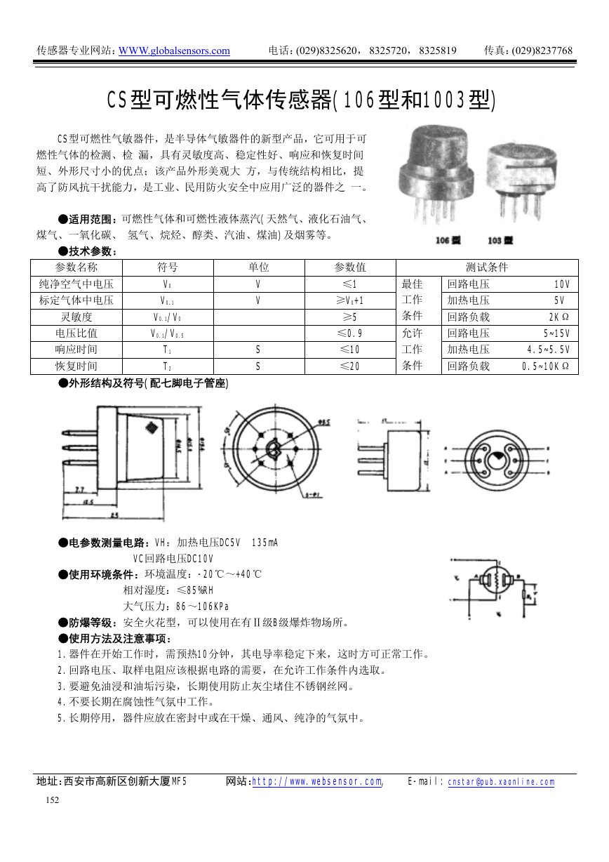 CS型可燃性气体传感器(106型和1003型)(传感器资料).pdf
 一种基于PWM的电压输出DAC电路设计.pdf
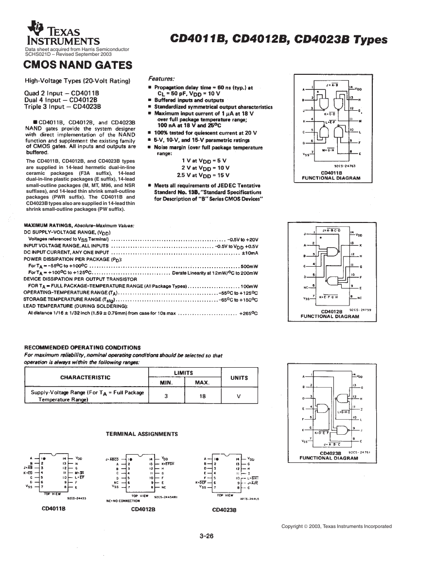 cd4011b(智能车电机驱动).pdf
 电路设计规范_中兴.pdf
 HA50-P(传感器资料).pdf
 ETD-core(TDK磁芯资料).pdf