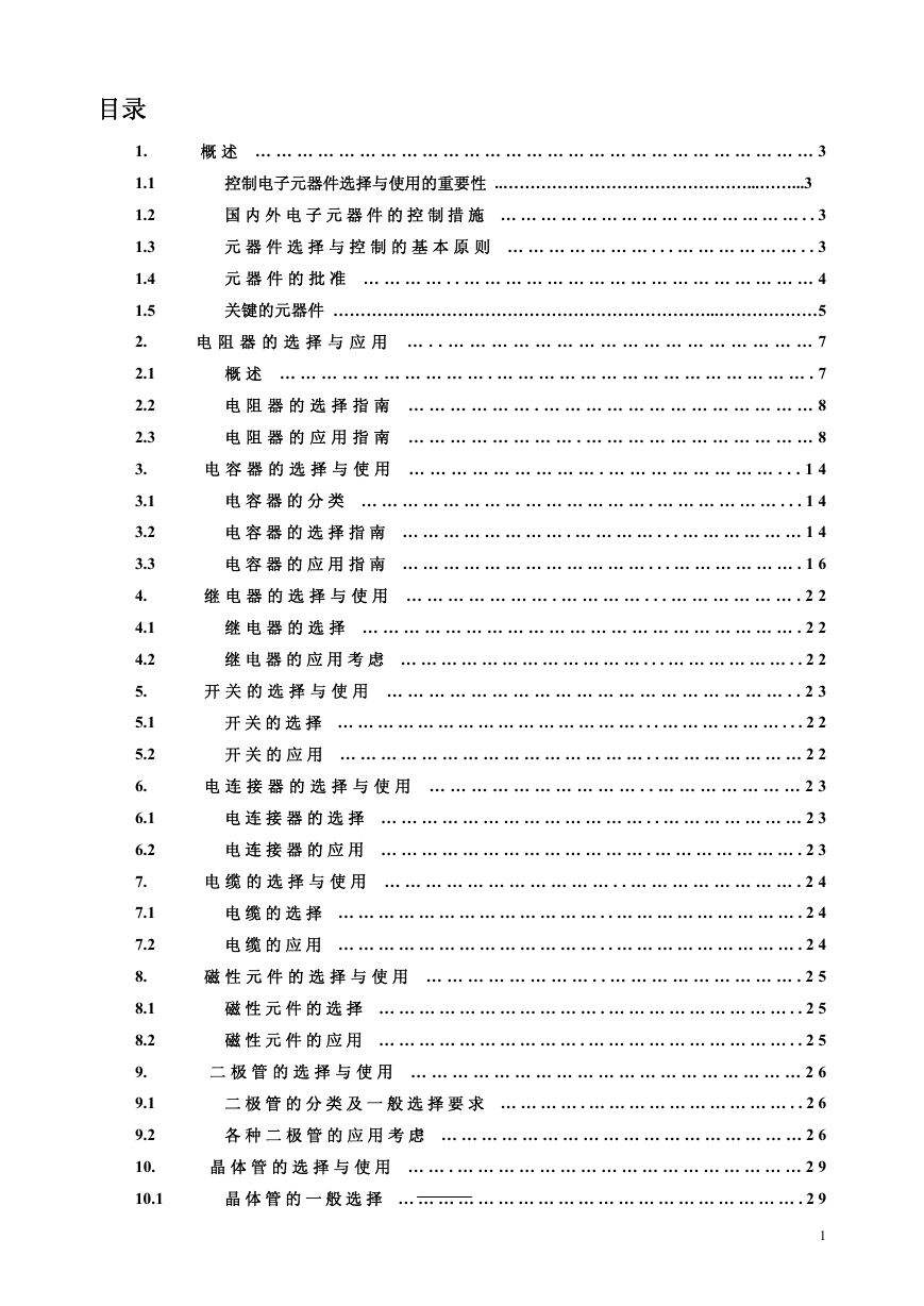
l Advanced Process Technology
l Ultra Low On-Resistance
l Dynamic dv/dt Rating
l 175°C Operating Temperature
l Fast Switching
l P-Channel
l Fully Avalanche Rated
Description
Fifth Generation HEXFETs from International Rectifier
utilize advanced processing techniques to achieve
extremely low on-resistance per silicon area. This
benefit, combined with the fast switching speed and
ruggedized device design that HEXFET Power
MOSFETs are well known for, provides the designer
with an extremely efficient and reliable device for use
in a wide variety of applications.
The TO-220 package is universally preferred for all
commercial-industrial applications at power
dissipation levels to approximately 50 watts. The low
thermal resistance and low package cost of the TO-
220 contribute to its wide acceptance throughout the
industry.
Absolute Maximum Ratings
ID @ TC = 25°C
ID @ TC = 100°C
IDM
PD @TC = 25°C
VGS
EAS
IAR
EAR
dv/dt
TJ
TSTG
Parameter
Continuous Drain Current, VGS @ -10V
Continuous Drain Current, VGS @ -10V
Pulsed Drain Current
Power Dissipation
Linear Derating Factor
Gate-to-Source Voltage
Single Pulse Avalanche Energy
Avalanche Current
Repetitive Avalanche Energy
Peak Diode Recovery dv/dt
Operating Junction and
Storage Temperature Range
Soldering Temperature, for 10 seconds
Mounting torque, 6-32 or M3 screw
Thermal Resistance
RθJC
RθCS
RθJA
Parameter
Junction-to-Case
Case-to-Sink, Flat, Greased Surface
Junction-to-Ambient
PD - 91280D
IRF4905
HEXFET® Power MOSFET
D
S
VDSS = -55V
RDS(on) = 0.02Ω
ID = -74A
G
TO-220AB
Max.
-74
-52
-260
200
1.3
± 20
930
-38
20
-5.0
-55 to + 175
300 (1.6mm from case )
10 lbfin (1.1Nm)
Typ.
0.50
Max.
0.75
62
Units
A
W
W/°C
V
mJ
A
mJ
V/ns
°C
Units
°C/W
05/24/07
�
IRF4905
Electrical Characteristics @ TJ = 25°C (unless otherwise specified)
Parameter
Drain-to-Source Breakdown Voltage
V(BR)DSS
∆V(BR)DSS/∆TJ Breakdown Voltage Temp. Coefficient
Static Drain-to-Source On-Resistance
RDS(on)
Gate Threshold Voltage
VGS(th)
gfs
Forward Transconductance
Drain-to-Source Leakage Current
Gate-to-Source Forward Leakage
Gate-to-Source Reverse Leakage
Total Gate Charge
Gate-to-Source Charge
Gate-to-Drain ("Miller") Charge
Turn-On Delay Time
Rise Time
Turn-Off Delay Time
Fall Time
IDSS
IGSS
Qg
Qgs
Qgd
td(on)
tr
td(off)
tf
LD
LS
Ciss
Coss
Crss
µA
n A
nC
V
Ω
V
S
Conditions
VGS = 0V, ID = -250µA
0.02
-4.0
-25
-250
100
-100
180
32
86
18
99
61
96
Min. Typ. Max. Units
-55
-0.05 V/°C Reference to 25°C, ID = -1mA
-2.0
21
VGS = -10V, ID = -38A
VDS = VGS, ID = -250µA
VDS = -25V, ID = -38A
VDS = -55V, VGS = 0V
VDS = -44V, VGS = 0V, TJ = 150°C
VGS = 20V
VGS = -20V
ID = -38A
VDS = -44V
VGS = -10V, See Fig. 6 and 13
VDD = -28V
ID = -38A
RG = 2.5Ω
RD = 0.72Ω, See Fig. 10
Between lead,
6mm (0.25in.)
from package
and center of die contact
VGS = 0V
VDS = -25V
= 1.0MHz, See Fig. 5
ns
G
D
S
Internal Drain Inductance
4.5
Internal Source Inductance
Input Capacitance
Output Capacitance
Reverse Transfer Capacitance
7.5
3400
1400
640
nH
pF
Source-Drain Ratings and Characteristics
Parameter
Min. Typ. Max. Units
Conditions
IS
ISM
VSD
trr
Qrr
ton
Continuous Source Current
(Body Diode)
Pulsed Source Current
(Body Diode)
Diode Forward Voltage
Reverse Recovery Time
Reverse Recovery Charge
Forward Turn-On Time
Notes:
Repetitive rating; pulse width limited by
max. junction temperature. ( See fig. 11 )
Starting TJ = 25°C, L = 1.3mH
RG = 25Ω, IAS = -38A. (See Figure 12)
-74
-260
89
230
-1.6
130
350
A
V
ns
nC
MOSFET symbol
showing the
integral reverse
p-n junction diode.
TJ = 25°C, IS = -38A, VGS = 0V
TJ = 25°C, IF = -38A
di/dt = -100A/µs
G
D
S
Intrinsic turn-on time is negligible (turn-on is dominated by LS+LD)
ISD ≤ -38A, di/dt ≤ -270A/µs, VDD ≤ V(BR)DSS,
TJ ≤ 175°C
Pulse width ≤ 300µs; duty cycle ≤ 2%.
�
IRF4905
-4.5V
1000
)
A
VGS
TOP - 15V
- 10V
- 8.0V
- 7.0V
- 6.0V
- 5.5V
- 5.0V
BOTTOM - 4.5V
(
t
n
e
r
r
u
C
e
c
r
u
o
S
-4.5V
-
o
i
t
-
n
a
r
D
,
I
-
D
100
10
1
0.1
1000
100
VGS
TOP - 15V
- 10V
- 8.0V
- 7.0V
- 6.0V
- 5.5V
- 5.0V
BOTTOM - 4.5V
)
A
(
t
n
e
r
r
u
C
e
c
r
u
o
S
-
o
10
i
t
-
n
a
r
D
,
I
-
D
1
0.1
20µs PULSE WIDTH
T = 25°C
c
A
100
1
10
-V , Drain-to-Source Voltage (V)
DS
20µs PULSE WIDTH
T = 175°C
C
A
100
1
10
-V , Drain-to-Source Voltage (V)
DS
Fig 1. Typical Output Characteristics
Fig 2. Typical Output Characteristics
1000
)
A
(
t
n
e
r
r
u
C
e
c
r
u
o
S
-
o
t
-
n
a
r
i
D
,
D
I
-
100
10
1
4
T = 25°C
J
T = 175°C
J
DS
V = -25V
20µs PULSE WIDTH
6
5
-V , Gate-to-Source Voltage (V)
7
8
9
GS
10
Fig 3. Typical Transfer Characteristics
2.0
I = -64A
D
e
c
n
a
)
d
e
z
i
l
a
m
r
o
N
(
i
t
s
s
e
R
n
O
e
c
r
u
o
S
-
o
i
t
-
n
a
r
D
)
n
o
(
,
S
D
R
A
1.5
1.0
0.5
0.0
-60 -40 -20
0
20
40
60
V = -10V
GS
A
80 100 120 140 160 180
JT , Junction Temperature (°C)
Fig 4. Normalized On-Resistance
Vs. Temperature
�
IRF4905
7000
6000
5000
4000
3000
2000
1000
)
F
p
(
e
c
n
a
t
i
c
a
p
a
C
,
C
V = 0V, f = 1MHz
GS
C = C + C , C SHORTED
iss gs gd ds
C = C
rss gd
C = C + C
oss ds gd
Ciss
Coss
Crss
0
1
10
A
100
-V , Drain-to-Source Voltage (V)
DS
)
V
(
e
g
a
t
l
o
V
e
c
r
u
o
S
-
o
t
t
-
e
a
G
,
S
G
V
-
20
16
12
8
4
0
I = -38A
D
V = -44V
V = -28V
DS
DS
FOR TEST CIRCUIT
SEE FIGURE 13
A
200
0
80
40
160
Q , Total Gate Charge (nC)
120
G
Fig 5. Typical Capacitance Vs.
Drain-to-Source Voltage
Fig 6. Typical Gate Charge Vs.
Gate-to-Source Voltage
1000
)
A
(
t
i
n
e
r
r
u
C
n
a
r
D
e
s
r
e
v
e
R
,
D
S
I
-
100
10
1
0.4
T = 175°C
J
T = 25°C
J
0.8
0.6
1.6
-V , Source-to-Drain Voltage (V)
1.0
1.2
1.4
SD
V = 0V
GS
A
1.8
)
A
(
t
n
e
r
r
u
C
n
a
r
i
D
,
I
-
D
1000
100
10
1
OPERATION IN THIS AREA LIMITED
BY RDS(on)
100µs
1ms
10ms
C
J
T = 25°C
T = 175°C
Single Pulse
1
10
-V , Drain-to-Source Voltage (V)
DS
A
100
Fig 7. Typical Source-Drain Diode
Fig 8. Maximum Safe Operating Area
Forward Voltage
�
)
A
(
t
n
e
r
r
u
C
n
a
r
D
i
,
I
D
80
60
40
20
0
25
50
75
150
T , Case Temperature ( C)
100
125
°
C
Fig 9. Maximum Drain Current Vs.
Case Temperature
1
0.1
D = 0.50
0.20
0.10
0.05
0.02
0.01
SINGLE PULSE
(THERMAL RESPONSE)
)
C
J
h
t
Z
(
e
s
n
o
p
s
e
R
l
a
m
r
e
h
T
IRF4905
RD
D.U.T.
VDD
-
+
VDS
VGS
RG
-10V
Pulse Width ≤ 1 µs
Duty Factor ≤ 0.1 %
Fig 10a. Switching Time Test Circuit
td(on)
tr
td(off)
tf
175
VGS
10%
90%
VDS
Fig 10b. Switching Time Waveforms
t
1
t
2
P
DM
2
thJC
+ T
C
Notes:
1. Duty factor D = t / t
1
x Z
2. Peak T = P
DM
J
0.01
0.00001
0.0001
0.001
0.01
0.1
1
t , Rectangular Pulse Duration (sec)
1
Fig 11. Maximum Effective Transient Thermal Impedance, Junction-to-Case
�
IRF4905
VDS
L
RG
-20V
tp
D.U.T
IAS
0.01Ω
VDD
A
DRIVER
15V
Fig 12a. Unclamped Inductive Test Circuit
IAS
tp
V(BR)DSS
Fig 12b. Unclamped Inductive Waveforms
QG
QGS
QGD
-10V
VG
D
I
TOP -16A
-27A
BOTTOM -38A
2500
2000
1500
1000
500
)
J
m
(
y
g
r
e
n
E
e
h
c
n
a
a
v
A
e
s
u
P
e
g
n
S
l
l
l
i
,
S
A
E
0
25
50
75
100
125
150
Starting T , Junction Temperature (°C)
J
A
175
Fig 12c. Maximum Avalanche Energy
Vs. Drain Current
Current Regulator
Same Type as D.U.T.
12V
.2µF
50KΩ
.3µF
VGS
-3mA
D.U.T.
-
VDS
+
Charge
IG
ID
Current Sampling Resistors
Fig 13a. Basic Gate Charge Waveform
Fig 13b. Gate Charge Test Circuit
�
IRF4905
Peak Diode Recovery dv/dt Test Circuit
D.U.T*
Circuit Layout Considerations
• Low Stray Inductance
• Ground Plane
• Low Leakage Inductance
Current Transformer
+
-
+
-
RG
VGS
+
-
• dv/dt controlled by RG
• ISD controlled by Duty Factor "D"
• D.U.T. - Device Under Test
+
-
V DD
* Reverse Polarity of D.U.T for P-Channel
Driver Gate Drive
P.W.
Period
D = P.W.
Period
D.U.T. ISD Waveform
Reverse
Recovery
Current
Re-Applied
Voltage
Body Diode Forward
Current
di/dt
D.U.T. VDS Waveform
Diode Recovery
dv/dt
Body Diode
Forward Drop
Inductor Curent
Ripple ≤ 5%
*** VGS = 5.0V for Logic Level and 3V Drive Devices
Fig 14. For P-Channel HEXFETS
[ ] ***
VGS=10V
[ ]
VDD
[ ]
ISD
�
IRF4905
TO-220AB Package Outline
Dimensions are shown in millimeters (inches)
TO-220AB Part Marking Information
(;$03/(� 7+,6�,6�$1�,5)�����
/27�&2'(�����
$66(0%/('�21�::���������
,1�7+(�$66(0%/<�/,1(��&�
,17(51$7,21$/
5(&7,),(5
/2*2
1RWH���3��LQ�DVVHPEO\�OLQH�SRVLWLRQ
LQGLFDWHV��/HDG���)UHH�
$66(0%/<
/27�&2'(
3$57�180%(5
'$7(�&2'(
<($5��� �����
:((.���
/,1(�&
TO-220AB packages are not recommended for Surface Mount Application.
Note: For the most current drawing please refer to IR website at http://www.irf.com/package/pkhexfet.html
Data and specifications subject to change without notice.
Qualification Standards can be found on IR’s Web site.
IR WORLD HEADQUARTERS: 233 Kansas St., El Segundo, California 90245, USA Tel: (310) 252-7105
TAC Fax: (310) 252-7903
Visit us at www.irf.com for sales contact information. 05/07
�

.pdf-第1页.png")
.pdf-第2页.png")
.pdf-第3页.png")
.pdf-第4页.png")
.pdf-第5页.png")
.pdf-第6页.png")
.pdf-第7页.png")
.pdf-第8页.png")
 Meta大模型论文:The Llama 3 Herd of Models.pdf
 ACS0709(传感器资料).PDF
 495个C语言常见问题集.pdf
 CS型可燃性气体传感器(106型和1003型)(传感器资料).pdf
 一种基于PWM的电压输出DAC电路设计.pdf
 cd4011b(智能车电机驱动).pdf
 电路设计规范_中兴.pdf
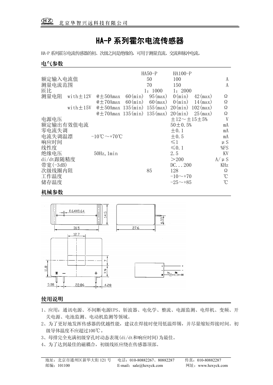 HA50-P(传感器资料).pdf
 ETD-core(TDK磁芯资料).pdf