Section I. MAX II Device Family Data
Sheet
This section provides designers with the data sheet specifications for MAX® II devices.
The chapters contain feature definitions of the internal architecture, Joint Test Action
Group (JTAG) and in-system programmability (ISP) information, DC operating
conditions, AC timing parameters, and ordering information for MAX II devices.
This section includes the following chapters:
■ Chapter 1, Introduction
■ Chapter 2, MAX II Architecture
■ Chapter 3, JTAG and In-System Programmability
■ Chapter 4, Hot Socketing and Power-On Reset in MAX II Devices
■ Chapter 5, DC and Switching Characteristics
■ Chapter 6, Reference and Ordering Information
Revision History
Refer to each chapter for its own specific revision history. For information about when
each chapter was updated, refer to the Chapter Revision Dates section, which appears
in the complete handbook.
© October 2008 Altera Corporation
MAX II Device Handbook
�
I–2
Section I: MAX II Device Family Data Sheet
Revision History
MAX II Device Handbook
© October 2008 Altera Corporation
�
MII51001-1.8
Introduction
Features
1. Introduction
The MAX® II family of instant-on, non-volatile CPLDs is based on a 0.18-µm, 6-layer-
metal-flash process, with densities from 240 to 2,210 logic elements (LEs) (128 to 2,210
equivalent macrocells) and non-volatile storage of 8 Kbits. MAX II devices offer high
I/O counts, fast performance, and reliable fitting versus other CPLD architectures.
Featuring MultiVolt core, a user flash memory (UFM) block, and enhanced in-system
programmability (ISP), MAX II devices are designed to reduce cost and power while
providing programmable solutions for applications such as bus bridging, I/O
expansion, power-on reset (POR) and sequencing control, and device configuration
control.
The MAX II CPLD has the following features:
■ Low-cost, low-power CPLD
■ Instant-on, non-volatile architecture
■ Standby current as low as 29 µA
■ Provides fast propagation delay and clock-to-output times
■ Provides four global clocks with two clocks available per logic array block (LAB)
■ UFM block up to 8 Kbits for non-volatile storage
■ MultiVolt core enabling external supply voltages to the device of either 3.3 V/2.5 V
or 1.8 V
■ MultiVolt I/O interface supporting 3.3-V, 2.5-V, 1.8-V, and 1.5-V logic levels
■ Bus-friendly architecture including programmable slew rate, drive strength, bus-
hold, and programmable pull-up resistors
■ Schmitt triggers enabling noise tolerant inputs (programmable per pin)
■ I/Os are fully compliant with the Peripheral Component Interconnect Special
Interest Group (PCI SIG) PCI Local Bus Specification, Revision 2.2 for 3.3-V
operation at 66 MHz
■ Supports hot-socketing
■ Built-in Joint Test Action Group (JTAG) boundary-scan test (BST) circuitry
compliant with IEEE Std. 1149.1-1990
■ ISP circuitry compliant with IEEE Std. 1532
© October 2008 Altera Corporation
MAX II Device Handbook
�
240
192
570
440
1,270
980
2,210
1,700
EPM240Z
EPM570Z
240
192
570
440
128 to 240
240 to 570
570 to 1,270
1,270 to 2,210
128 to 240
240 to 570
8,192
80
4.7
304
1.7
4.3
8,192
160
5.4
304
1.2
4.5
8,192
212
6.2
304
1.2
4.6
8,192
272
7.0
304
1.2
4.6
8,192
80
7.5
152
2.3
6.5
8,192
160
9.0
152
2.2
6.7
LEs
Typical Equivalent Macrocells
Equivalent Macrocell Range
UFM Size (bits)
Maximum User I/O pins
tPD1 (ns) (1)
fCNT (MHz) (2)
tSU (ns)
tCO (ns)
Notes to Table 1–1:
(1)
1–2
Chapter 1: Introduction
Features
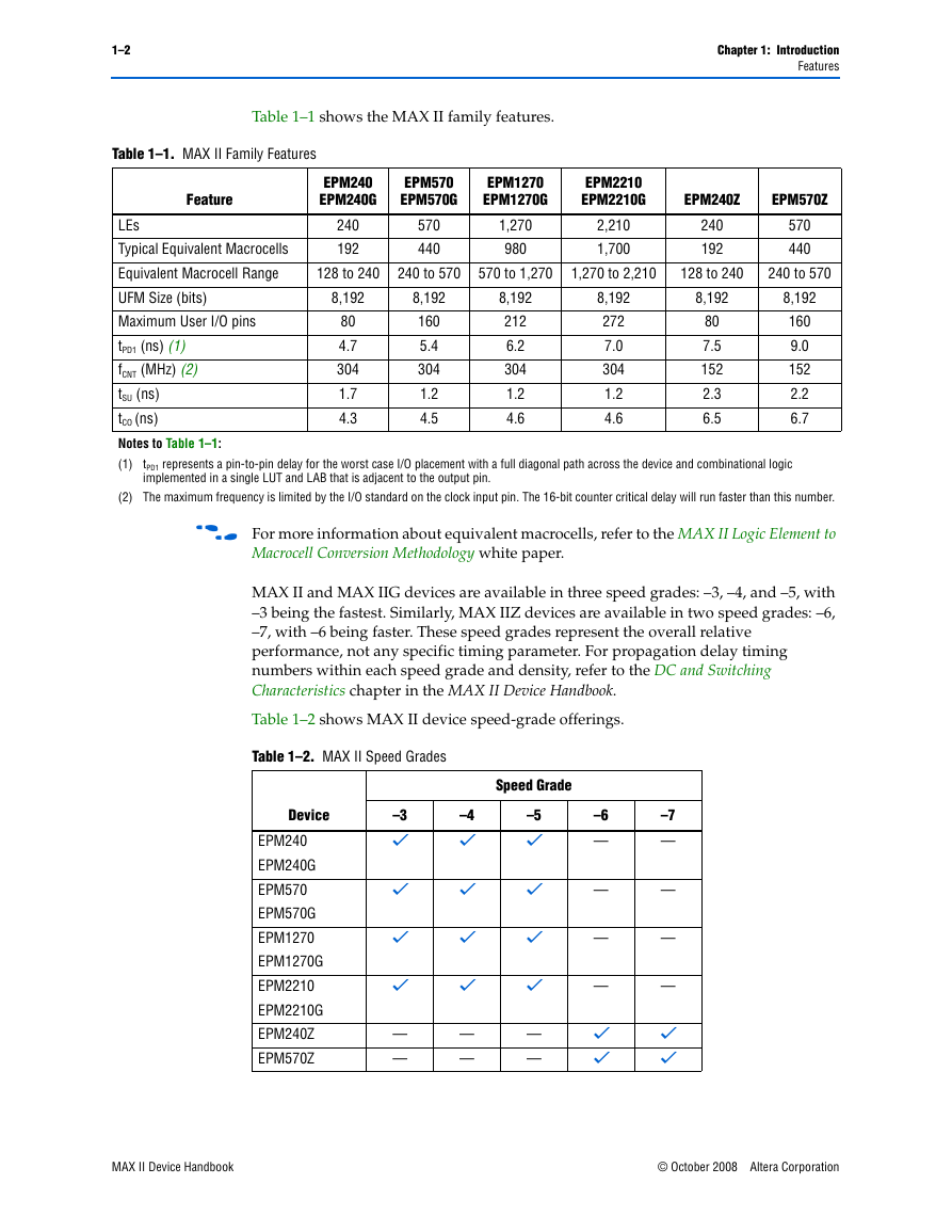
Table 1–1 shows the MAX II family features.
Table 1–1. MAX II Family Features
Feature
EPM240
EPM240G
EPM570
EPM570G
EPM1270
EPM1270G
EPM2210
EPM2210G
tPD1 represents a pin-to-pin delay for the worst case I/O placement with a full diagonal path across the device and combinational logic
implemented in a single LUT and LAB that is adjacent to the output pin.
(2) The maximum frequency is limited by the I/O standard on the clock input pin. The 16-bit counter critical delay will run faster than this number.
f For more information about equivalent macrocells, refer to the MAX II Logic Element to
Macrocell Conversion Methodology white paper.
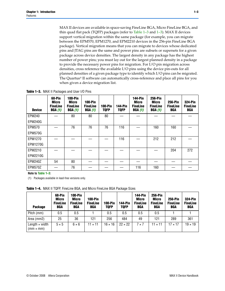
MAX II and MAX IIG devices are available in three speed grades: –3, –4, and –5, with
–3 being the fastest. Similarly, MAX IIZ devices are available in two speed grades: –6,
–7, with –6 being faster. These speed grades represent the overall relative
performance, not any specific timing parameter. For propagation delay timing
numbers within each speed grade and density, refer to the DC and Switching
Characteristics chapter in the MAX II Device Handbook.
Table 1–2 shows MAX II device speed-grade offerings.
Table 1–2. MAX II Speed Grades
Speed Grade
Device
EPM240
EPM240G
EPM570
EPM570G
EPM1270
EPM1270G
EPM2210
EPM2210G
EPM240Z
EPM570Z
–3
v
v
v
v
—
—
–4
v
v
v
v
—
—
–5
v
v
v
v
—
—
–6
—
—
—
—
v
v
–7
—
—
—
—
v
v
MAX II Device Handbook
© October 2008 Altera Corporation
�
Chapter 1: Introduction
Features
1–3
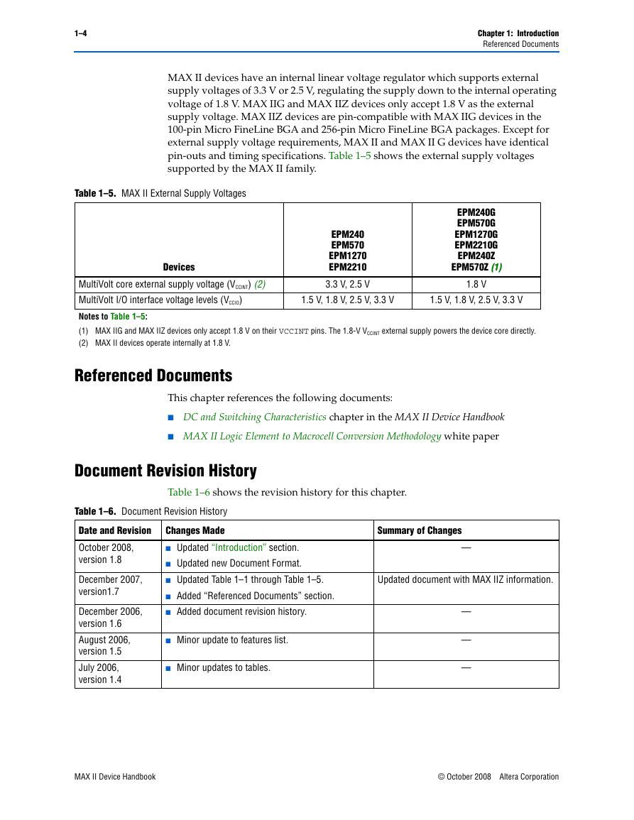
MAX II devices are available in space-saving FineLine BGA, Micro FineLine BGA, and
thin quad flat pack (TQFP) packages (refer to Table 1–3 and 1–3). MAX II devices
support vertical migration within the same package (for example, you can migrate
between the EPM570, EPM1270, and EPM2210 devices in the 256-pin FineLine BGA
package). Vertical migration means that you can migrate to devices whose dedicated
pins and JTAG pins are the same and power pins are subsets or supersets for a given
package across device densities. The largest density in any package has the highest
number of power pins; you must lay out for the largest planned density in a package
to provide the necessary power pins for migration. For I/O pin migration across
densities, cross reference the available I/O pins using the device pin-outs for all
planned densities of a given package type to identify which I/O pins can be migrated.
The Quartus® II software can automatically cross-reference and place all pins for you
when given a device migration list.
Table 1–3. MAX II Packages and User I/O Pins
68-Pin
Micro
FineLine
BGA (1)
100-Pin
Micro
FineLine
BGA (1)
100-Pin
FineLine
BGA (1)
Device
80
76
—
—
EPM240
EPM240G
EPM570
EPM570G
EPM1270
EPM1270G
EPM2210
EPM2210G
EPM240Z
EPM570Z
Note to Table 1–3:
(1) Packages available in lead-free versions only.
80
76
54
—
—
—
—
—
80
76
—
—
—
—
100-Pin
TQFP
80
144-Pin
TQFP
—
76
—
—
—
—
116
116
—
—
—
144-Pin
Micro
FineLine
BGA (1)
256-Pin
Micro
FineLine
BGA (1)
—
—
—
—
—
116
—
160
212
—
—
160
256-Pin
FineLine
BGA
—
324-Pin
FineLine
BGA
—
160
212
204
—
—
—
—
272
—
—
Table 1–4. MAX II TQFP, FineLine BGA, and Micro FineLine BGA Package Sizes
68-Pin
Micro
FineLine
BGA
0.5
25
5 × 5
100-Pin
Micro
FineLine
BGA
0.5
36
6 × 6
100-Pin
FineLine
BGA
1
121
100-Pin
TQFP
0.5
256
144-Pin
TQFP
0.5
484
11 × 11
16 × 16
22 × 22
144-Pin
Micro
FineLine
BGA
0.5
49
7 × 7
256-Pin
Micro
FineLine
BGA
0.5
121
256-Pin
FineLine
BGA
1
289
324-Pin
FineLine
BGA
1
361
11 × 11
17 × 17
19 × 19
Package
Pitch (mm)
Area (mm2)
Length × width
(mm × mm)
© October 2008 Altera Corporation
MAX II Device Handbook
�
1–4
Chapter 1: Introduction
Referenced Documents
MAX II devices have an internal linear voltage regulator which supports external
supply voltages of 3.3 V or 2.5 V, regulating the supply down to the internal operating
voltage of 1.8 V. MAX IIG and MAX IIZ devices only accept 1.8 V as the external
supply voltage. MAX IIZ devices are pin-compatible with MAX IIG devices in the
100-pin Micro FineLine BGA and 256-pin Micro FineLine BGA packages. Except for
external supply voltage requirements, MAX II and MAX II G devices have identical
pin-outs and timing specifications. Table 1–5 shows the external supply voltages
supported by the MAX II family.
Table 1–5. MAX II External Supply Voltages
Devices
EPM240
EPM570
EPM1270
EPM2210
3.3 V, 2.5 V
EPM240G
EPM570G
EPM1270G
EPM2210G
EPM240Z
EPM570Z (1)
1.8 V
MultiVolt core external supply voltage (VCCINT) (2)
MultiVolt I/O interface voltage levels (VCCIO)
Notes to Table 1–5:
(1) MAX IIG and MAX IIZ devices only accept 1.8 V on their VCCINT pins. The 1.8-V VCCINT external supply powers the device core directly.
(2) MAX II devices operate internally at 1.8 V.
1.5 V, 1.8 V, 2.5 V, 3.3 V
1.5 V, 1.8 V, 2.5 V, 3.3 V
Referenced Documents
This chapter references the following documents:
■ DC and Switching Characteristics chapter in the MAX II Device Handbook
■ MAX II Logic Element to Macrocell Conversion Methodology white paper
Document Revision History
Table 1–6 shows the revision history for this chapter.
Table 1–6. Document Revision History
Date and Revision
October 2008,
version 1.8
December 2007,
version1.7
December 2006,
version 1.6
August 2006,
version 1.5
July 2006,
version 1.4
Changes Made
■ Updated “Introduction” section.
■ Updated new Document Format.
■ Updated Table 1–1 through Table 1–5.
■ Added “Referenced Documents” section.
■ Added document revision history.
■ Minor update to features list.
■ Minor updates to tables.
Summary of Changes
—
Updated document with MAX IIZ information.
—
—
—
MAX II Device Handbook
© October 2008 Altera Corporation
�
Chapter 1: Introduction
Document Revision History
1–5
Table 1–6. Document Revision History
Date and Revision
June 2005,
version 1.3
December 2004,
version 1.2
June 2004,
version 1.1
Changes Made
■ Updated timing numbers in Table 1-1.
■ Updated timing numbers in Table 1-1.
■ Updated timing numbers in Table 1-1.
Summary of Changes
—
—
—
© October 2008 Altera Corporation
MAX II Device Handbook
�
1–6
Chapter 1: Introduction
Document Revision History
MAX II Device Handbook
© October 2008 Altera Corporation
�


