SD Card Specification
Simplified Version of:
Part E1
Secure Digital Input/Output
(SDIO)
Card Specification
Version 1.00
October 2001
SD Association
Copyright 2000, 2001 SD Association
�
SDIO Simple Specification Version 1.0 DO NOT COPY ©Copyright SD Association, 2000, 2001
Version
1.0
Changes compared to previous issue
Revision History
Date
Base version initial release
October, 2001
Conditions for publication
Publisher and Copyright Holder:
SD Association
719 San Benito St. Suite C
Hollister, CA 95023
USA
Phone: +1 831 636 7322
Fax: +1 831 623 2248
E-mail: president@sdcard.org
Confidentiality:
This document is a simplified version of the original. This version is not required to be treated as confidential
and Non Disclosure Agreement with neither the 3C LLC nor the SDA is required.
Reproduction in whole or in part is prohibited without prior written permission of SDA.
Exemption:
None will be liable for any damages from use of this document.
Important additional information!
The reader is directed to the additional information available in section Error! Reference source not found..
This information will inform the reader of changes to the SDIO specification proposed for the next revision of
this specification that should be considered in the design of any SDIO device.
l
�
SDIO Simple Specification Version 1.0 DO NOT COPY ©Copyright SD Association, 2000, 2001
Table of Contents
5.1
5.2
5.2.1
2.2.1
2.2.2
2.2.3
1. General Description.......................................................................................................................................1
1.1 SDIO features.........................................................................................................................................1
1.2 Primary Reference Document................................................................................................................1
2. SDIO Signaling Definition..............................................................................................................................2
2.1 SDIO Card Types ...................................................................................................................................2
2.2 SDIO Card modes..................................................................................................................................2
SPI (Card mandatory support)........................................................................................................2
1-bit SD data transfer mode (Card mandatory support).................................................................2
4-bit SD data transfer mode (mandatory for High-Speed cards, optional for Low-Speed) ............2
2.3 SDIO Host Modes ..................................................................................................................................2
2.4 Signal Pins..............................................................................................................................................3
2.5 Host Requirements for SDIO .................................................................................................................3
3. SDIO Card Initialization .................................................................................................................................4
3.1 Differences in I/O card initialization........................................................................................................4
4. Differences with SD Memory Specification ...................................................................................................7
4.1 Unsupported SD Memory commands....................................................................................................7
4.2 Bus Width ...............................................................................................................................................8
4.3 Card Detect Resistor..............................................................................................................................8
4.4 Data Transfer Abort ................................................................................................................................8
4.5 Changes to SD Memory Fixed Registers...............................................................................................8
4.5.1 OCR Register..................................................................................................................................8
CID Register....................................................................................................................................8
4.5.2
4.5.3
RCA Register ..................................................................................................................................8
5. New I/O Read/Write Commands ...................................................................................................................9
IO_RW_DIRECT command (CMD52)....................................................................................................9
IO_RW_EXTENDED command (CMD53) .............................................................................................9
CMD53 Data Transfer Format.........................................................................................................9
6. SDIO Card Internal Operation.....................................................................................................................10
6.1 Overview...............................................................................................................................................10
6.2 Register Access Time...........................................................................................................................10
6.3
Interrupts ..............................................................................................................................................10
6.4 Suspend/Resume................................................................................................................................. 11
6.5 Read Wait (Optional)............................................................................................................................ 11
6.6 SDIO Fixed Internal Map......................................................................................................................12
6.7 Common I/O Area (CIA).......................................................................................................................12
6.8 Card Common Control Registers (CCCR)...........................................................................................13
6.9
Function Basic Registers (FBR)...........................................................................................................13
Card Information Structure (CIS)......................................................................................................13
6.10
Multiple Function SD Cards..............................................................................................................13
6.11
6.12
Embedded I/O Code Storage Area (CSA)........................................................................................13
7. SDIO Interrupts............................................................................................................................................14
Interrupt Timing ....................................................................................................................................14
SPI and SD 1-bit mode interrupts.................................................................................................14
SD 4-bit mode ...............................................................................................................................14
Interrupt Clear Timing ...................................................................................................................14
8. SDIO Physical Properties............................................................................................................................15
8.1 SDIO Size.............................................................................................................................................15
8.2 SDIO Card Package.............................................................................................................................15
9. SDIO Mechanical Extensions......................................................................................................................16
9.1 Additional ESD/EMI Ground Point .......................................................................................................16
9.2 Extended Case.....................................................................................................................................16
9.3 Write Protect Switch.............................................................................................................................16
10. SDIO Power .............................................................................................................................................18
SDIO Card Initialization Voltage .......................................................................................................18
7.1.1
7.1.2
7.1.3
7.1
10.1
i
�
SDIO Simple Specification Version 1.0 DO NOT COPY ©Copyright SD Association, 2000, 2001
10.2
10.3
SDIO Power Consumption ...............................................................................................................18
SDIO Current....................................................................................................................................18
11.
Abbreviations and Terms .........................................................................................................................19
A.1 SD and SPI Command List........................................................................................................................A
B.1 Normative References .............................................................................................................................. C
C.1 Example SDIO Controller Design ............................................................................................................. D
Table of Tables
Table 1 SDIO pin definitions .................................................................................................................................3
Table 2 Unsupported SD Memory Commands.....................................................................................................7
Table 3 SDIO exceptions to SD physical section 8.1 requirements...................................................................15
Table 4 SD Mode Command List..........................................................................................................................A
Table 5 SPI Mode Command List .........................................................................................................................B
Table of Figures
Figure 1 Signal connection to two 4-bit SDIO cards ............................................................................................3
Figure 2 Card initialization flow in SD mode (SDIO aware host) .........................................................................5
Figure 3 Card initialization flow in SPI mode (SDIO aware host).........................................................................6
Figure 4 SDIO Internal Map................................................................................................................................12
Figure 5 SDIO Mechanical Extensions...............................................................................................................17
Figure 6 SDIO Internal State Machine example.................................................................................................. D
Figure 7 State Diagram for Bus State Machine ................................................................................................... D
Figure 8 State Diagram for Function State Machine.............................................................................................E
ii
�
SDIO Simple Specification Version 1.0 DO NOT COPY ©Copyright SD Association, 2000, 2001
1. General Description
The SDIO (Secure Digital I/O) card is based on and compatible with the SD memory card. This compatibility
includes mechanical, electrical, power, signaling and software. The intent of the SDIO card is to provide
high-speed data I/O with low power consumption for mobile electronic devices. A primary goal is that an SDIO
card inserted into a non-SDIO aware host will cause no physical damage or disruption of that device or it’s
software. In this case, the SDIO card should simply be ignored. Once inserted into an SDIO aware host, the
detection of the card will be via the normal means described in the SD specification with some extensions. In
this state, the SDIO card will be idle and draw a small amount of power (15 mA averaged over 1 second).
During the normal initialization and interrogation of the card by the host, the card will identify itself as an SDIO
device. The host software will then obtain the card information in a tuple (linked list) format and determine if
that card’s I/O function(s) are acceptable to activate. This decision will be based on such parameters as power
requirements or the availability of appropriate software drivers. If the card is acceptable, it will be allowed to
power up fully and start the I/O function(s) built into it.
1.1
SDIO features
� Targeted for portable and stationary applications
� Minimal or no modification to SD Physical bus is required
� Minimal change to memory driver software
� Extended physical form factor available for specialized applications
� Plug and play (PnP) support
� Multi-function support including multiple I/O and combined I/O and memory
� Up to 7 I/O functions plus one memory supported on one card.
� Allows card to interrupt host
� Initialization Voltage: 2.0 to 3.6V
� Operational Voltage range: 3.1 to 3.5V
Primary Reference Document
1.2
This spec is based on and refers extensively to the SDA document:
SD Memory Card Specifications
Part 1
PHYSICAL LAYER SPECIFICATION
September 2000
Version 1.01
The reader is directed to this document for more information on the basic operation of SD devices. In addition,
other documents are referenced in this specification. A complete list can be found in section B.1.
1
�
SDIO Simple Specification Version 1.0 DO NOT COPY ©Copyright SD Association, 2000, 2001
SDIO Card Types
2. SDIO Signaling Definition
2.1
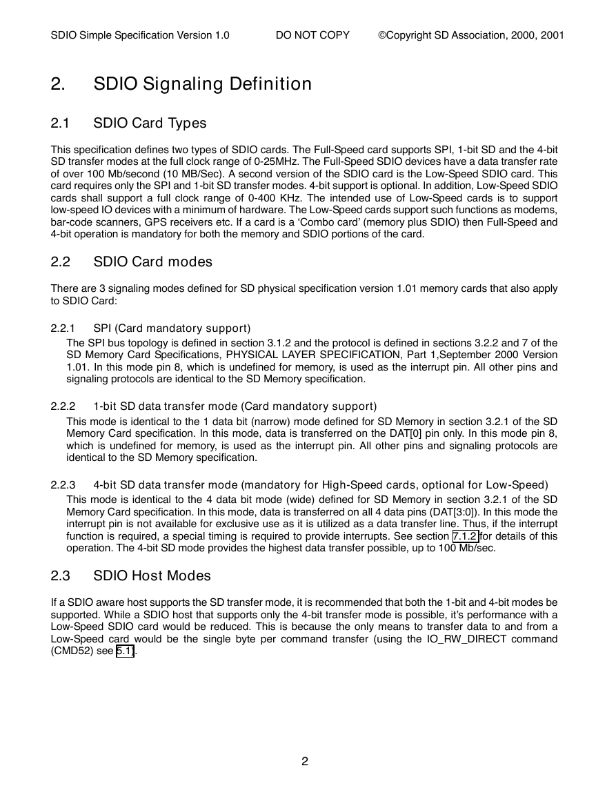
This specification defines two types of SDIO cards. The Full-Speed card supports SPI, 1-bit SD and the 4-bit
SD transfer modes at the full clock range of 0-25MHz. The Full-Speed SDIO devices have a data transfer rate
of over 100 Mb/second (10 MB/Sec). A second version of the SDIO card is the Low-Speed SDIO card. This
card requires only the SPI and 1-bit SD transfer modes. 4-bit support is optional. In addition, Low-Speed SDIO
cards shall support a full clock range of 0-400 KHz. The intended use of Low-Speed cards is to support
low-speed IO devices with a minimum of hardware. The Low-Speed cards support such functions as modems,
bar-code scanners, GPS receivers etc. If a card is a ‘Combo card’ (memory plus SDIO) then Full-Speed and
4-bit operation is mandatory for both the memory and SDIO portions of the card.
2.2
There are 3 signaling modes defined for SD physical specification version 1.01 memory cards that also apply
to SDIO Card:
2.2.1
SPI (Card mandatory support)
SDIO Card modes
The SPI bus topology is defined in section 3.1.2 and the protocol is defined in sections 3.2.2 and 7 of the
SD Memory Card Specifications, PHYSICAL LAYER SPECIFICATION, Part 1,September 2000 Version
1.01. In this mode pin 8, which is undefined for memory, is used as the interrupt pin. All other pins and
signaling protocols are identical to the SD Memory specification.
1-bit SD data transfer mode (Card mandatory support)
This mode is identical to the 1 data bit (narrow) mode defined for SD Memory in section 3.2.1 of the SD
Memory Card specification. In this mode, data is transferred on the DAT[0] pin only. In this mode pin 8,
which is undefined for memory, is used as the interrupt pin. All other pins and signaling protocols are
identical to the SD Memory specification.
2.2.2
2.2.3
4-bit SD data transfer mode (mandatory for High-Speed cards, optional for Low-Speed)
This mode is identical to the 4 data bit mode (wide) defined for SD Memory in section 3.2.1 of the SD
Memory Card specification. In this mode, data is transferred on all 4 data pins (DAT[3:0]). In this mode the
interrupt pin is not available for exclusive use as it is utilized as a data transfer line. Thus, if the interrupt
function is required, a special timing is required to provide interrupts. See section 7.1.2 for details of this
operation. The 4-bit SD mode provides the highest data transfer possible, up to 100 Mb/sec.
SDIO Host Modes
2.3
If a SDIO aware host supports the SD transfer mode, it is recommended that both the 1-bit and 4-bit modes be
supported. While a SDIO host that supports only the 4-bit transfer mode is possible, it’s performance with a
Low-Speed SDIO card would be reduced. This is because the only means to transfer data to and from a
Low-Speed card would be the single byte per command transfer (using the IO_RW_DIRECT command
(CMD52) see 5.1).
2
�
SDIO Simple Specification Version 1.0 DO NOT COPY ©Copyright SD Association, 2000, 2001
2.4
Signal Pins
SD Host
CLK
CMD
DAT[3:0]
CLK
CMD
DAT[3:0]
SD I/O Card
SD I/O Card
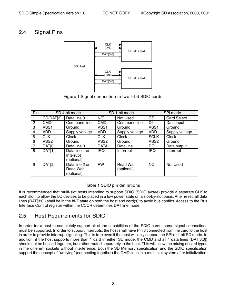
Figure 1 Signal connection to two 4-bit SDIO cards
Pin
1
2
3
4
5
6
7
8
SD 4-bit mode
CD/DAT[3] Data line 3
CMD
VSS1
VDD
CLK
VSS2
DAT[0]
DAT[1]
N/C
Command line CMD
Ground
VSS1
Supply voltage VDD
CLK
Clock
Ground
VSS2
DATA
Data line 0
Data line 1 or
IRQ
Interrupt
(optional)
Data line 2 or
Read Wait
(optional)
SD 1-bit mode
Not Used
CS
Command line DI
Ground
VSS1
Supply voltage VDD
SCLK
Clock
Ground
VSS2
DO
Data line
Interrupt
IRQ
SPI mode
Card Select
Data input
Ground
Supply voltage
Clock
Ground
Data output
Interrupt
9
DAT[2]
RW
Read Wait
(optional)
NC
Not Used
Table 1 SDIO pin definitions
It is recommended that multi-slot hosts intending to support SDIO (SDIO aware) provide a separate CLK to
each slot, to allow the I/O devices to be placed in a low power state on a slot-by-slot basis. After reset, all data
lines (DAT[3:0]) shall be in the hi-Z state on both the host and card(s) to avoid bus conflict. Access to the Bus
Interface Control register within the CCCR determines DAT line mode.
2.5 Host Requirements for SDIO
In order for a host to completely support all of the capabilities of the SDIO cards, some signal connections
must be supported. In order to support interrupts, the host shall have Pin 8 connected from the card to the host
in order to provide interrupt signaling. This is true even if the host will only support the SPI or 1 bit SD mode. In
addition, if the host supports more than 1 card in either SD mode, the CMD and all 4 data lines (DAT[3:0])
should not be bussed together, but rather routed separately to the host. This will allow the mixing of card types
in the different sockets without interference. Both the SD Memory specification and the SDIO specification
support the concept of “unifying” (connecting together) the CMD lines in a multi-slot system after initialization.
3
�
SDIO Simple Specification Version 1.0 DO NOT COPY ©Copyright SD Association, 2000, 2001
3. SDIO Card Initialization
3.1 Differences in I/O card initialization
A requirement for the SDIO specification is that an SDIO card must not cause non-I/O aware hosts to fail when
inserted. In order to prevent operation of I/O Functions in non-I/O aware hosts, a change to the SD card
identification mode flowchart is needed. A new command (IO_SEND_OP_COND, CMD5) is added to replace
the ACMD41 for SDIO initialization by I/O aware hosts.
After reset or power-up, all I/O functions on the card are disabled and the I/O portion of the card will not
respond to any operation except CMD5 or CMD0 with CS=low. If there is SD memory installed on the card
(also called a combo card), that memory will respond normally to all normal mandatory memory commands.
An I/O only card will not respond to the ACMD41 and thus appear initially as an MMC card (See B.1 for
information on the MMC specification). The I/O only card will also not respond to the CMD1 used to initialize
the MMC cards and appear as a non-responsive card. The host will then give up and disable this device Thus,
the non-aware host will receive no response from an I/O only card and force it to the inactive state.
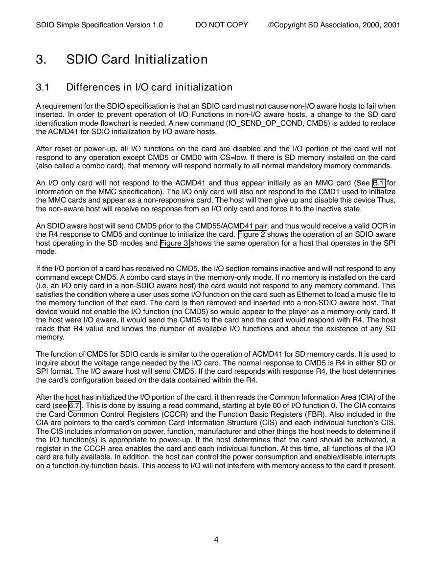
An SDIO aware host will send CMD5 prior to the CMD55/ACMD41 pair, and thus would receive a valid OCR in
the R4 response to CMD5 and continue to initialize the card. Figure 2 shows the operation of an SDIO aware
host operating in the SD modes and Figure 3 shows the same operation for a host that operates in the SPI
mode.
If the I/O portion of a card has received no CMD5, the I/O section remains inactive and will not respond to any
command except CMD5. A combo card stays in the memory-only mode. If no memory is installed on the card
(i.e. an I/O only card in a non-SDIO aware host) the card would not respond to any memory command. This
satisfies the condition where a user uses some I/O function on the card such as Ethernet to load a music file to
the memory function of that card. The card is then removed and inserted into a non-SDIO aware host. That
device would not enable the I/O function (no CMD5) so would appear to the player as a memory-only card. If
the host were I/O aware, it would send the CMD5 to the card and the card would respond with R4. The host
reads that R4 value and knows the number of available I/O functions and about the existence of any SD
memory.
The function of CMD5 for SDIO cards is similar to the operation of ACMD41 for SD memory cards. It is used to
inquire about the voltage range needed by the I/O card. The normal response to CMD5 is R4 in either SD or
SPI format. The I/O aware host will send CMD5. If the card responds with response R4, the host determines
the card’s configuration based on the data contained within the R4.
After the host has initialized the I/O portion of the card, it then reads the Common Information Area (CIA) of the
card (see 6.7). This is done by issuing a read command, starting at byte 00 of I/O function 0. The CIA contains
the Card Common Control Registers (CCCR) and the Function Basic Registers (FBR). Also included in the
CIA are pointers to the card’s common Card Information Structure (CIS) and each individual function’s CIS.
The CIS includes information on power, function, manufacturer and other things the host needs to determine if
the I/O function(s) is appropriate to power-up. If the host determines that the card should be activated, a
register in the CCCR area enables the card and each individual function. At this time, all functions of the I/O
card are fully available. In addition, the host can control the power consumption and enable/disable interrupts
on a function-by-function basis. This access to I/O will not interfere with memory access to the card if present.
4
�
