RFX2401C
Production Data Sheet
CMOS 2.4GHZ ZIGBEE/ISM TRANSMIT/RECEIVE RFeIC
Description
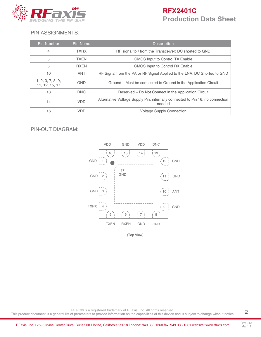
The RFX2401C is a fully integrated, single-chip, single-die RFeIC (RF Front-end
Integrated Circuit) which incorporates all the RF functionality needed for IEEE
802.15.4/ZigBee, wireless sensor network, and any other wireless systems in the
2.4GHz ISM band. The RFX2401C architecture integrates the PA, LNA, Transmit
and Receive switching circuitry, the associated matching network, and the
harmonic filter all in a CMOS single-chip device.
Typical high power applications include home and industrial automation, smart
power, and RF4CE among others. Combining superior performance, high
sensitivity and efficiency, low noise, small form factor, and low cost, RFX2401C
is the perfect solution for applications requiring extended range and bandwidth.
RFX2401C has simple and low-voltage CMOS control logic, and requires
minimal external components for system implementation.
Applications
ZigBee Extended Range Devices
ZigBee Smart Power
Mobile and Battery ZigBee Systems
Home and Industrial Automation
RF4CE Remote Control
Custom 2.4GHz Radio Systems
FEATURES
2.4GHz ZigBee High Power Single-Chip, Single-Die
ESD Protection Circuitry on All Ports
RF Front-End IC
Combined TX / RX Transceiver Port and Single
Antenna Port
2.4GHz Transmit High Power Amplifier with Low-
Pass Harmonic Filter
Low Noise Amplifier
DC Decoupled RF Ports
Internal RF Decoupling on All VDD Bias Pins
Low Noise Figure for the Receive Channel
Very Low DC Power Consumption
Full On-chip Matching and Decoupling Circuitry
Transmit / Receive Switch Circuitry
Minimal External Components Required
High Transmit Signal Linearity Meeting Standards for
50-Ohm Input / Output Matching
OQPSK Modulation
Integrated Power Detector for Transmit Power
Monitor and Control
Low Voltage (1.2V) CMOS Control Logic
Market Proven CMOS Technology
3 x 3 x 0.55mm Small Outline QFN-16 Package with
Exposed Ground Pad
This product document is a general list of parameters to provide information on the capabilities of this device and is subject to change without notice.
RFeIC® is a registered trademark of RFaxis, Inc. All rights reserved.
RFaxis, Inc. | 7595 Irvine Center Drive, Suite 200 | Irvine, California 92618 | phone: 949.336.1360 fax: 949.336.1361 website: www.rfaxis.com
1
Rev 2.5c
Mar '12
hot
GNDGND12341211109151614135678GND17GNDGNDGNDGNDDNCGNDVDDVDDGNDTXRXGNDANTRXENTXEN�
RFX2401C
Production Data Sheet
PIN ASSIGNMENTS:
Pin Number
Pin Name
Description
4
5
6
10
TXRX
TXEN
RXEN
RF signal to / from the Transceiver: DC shorted to GND
CMOS Input to Control TX Enable
CMOS Input to Control RX Enable
ANT
RF Signal from the PA or RF Signal Applied to the LNA; DC Shorted to GND
1, 2, 3, 7, 8, 9,
11, 12, 15, 17
13
14
16
GND
DNC
VDD
VDD
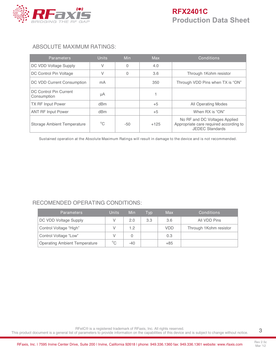
PIN-OUT DIAGRAM:
Ground – Must be connected to Ground in the Application Circuit
Reserved – Do Not Connect in the Application Circuit
Alternative Voltage Supply Pin, internally connected to Pin 16, no connection
needed
Voltage Supply Connection
(Top View)
This product document is a general list of parameters to provide information on the capabilities of this device and is subject to change without notice.
RFeIC® is a registered trademark of RFaxis, Inc. All rights reserved.
RFaxis, Inc. | 7595 Irvine Center Drive, Suite 200 | Irvine, California 92618 | phone: 949.336.1360 fax: 949.336.1361 website: www.rfaxis.com
2
Rev 2.5c
Mar '12
16512341514136789101112GNDGNDGNDTXRXTXENGNDVDDGNDGNDANTGNDRXENGNDDNCVDD17GNDGND�
RFX2401C
Production Data Sheet
Max
4.0
3.6
350
1
+5
+5
Conditions
Through 1Kohm resistor
Through VDD Pins when TX is “ON”
All Operating Modes
When RX is “ON”
-50
+125
No RF and DC Voltages Applied
Appropriate care required according to
JEDEC Standards
ABSOLUTE MAXIMUM RATINGS:
Parameters
Units
Min
DC VDD Voltage Supply
DC Control Pin Voltage
V
V
DC VDD Current Consumption
mA
DC Control Pin Current
Consumption
TX RF Input Power
ANT RF Input Power
Storage Ambient Temperature
μA
dBm
dBm
oC
0
0
Sustained operation at the Absolute Maximum Ratings will result in damage to the device and is not recommended.
RECOMENDED OPERATING CONDITIONS:
Parameters
Units
Min
Typ
DC VDD Voltage Supply
Control Voltage “High”
Control Voltage “Low”
Operating Ambient Temperature
V
V
V
oC
2.0
1.2
0
-40
3.3
Max
3.6
VDD
0.3
+85
Conditions
All VDD Pins
Through 1Kohm resistor
This product document is a general list of parameters to provide information on the capabilities of this device and is subject to change without notice.
RFeIC® is a registered trademark of RFaxis, Inc. All rights reserved.
RFaxis, Inc. | 7595 Irvine Center Drive, Suite 200 | Irvine, California 92618 | phone: 949.336.1360 fax: 949.336.1361 website: www.rfaxis.com
3
Rev 2.5c
Mar '12
�
RFX2401C
Production Data Sheet
TRANSMIT TECHNICAL PARAMETERS (VDD=3.3V; T=+25 oC)
Parameters
Units
Min
Typ
Max
Conditions
Operating Frequency Band
Saturated Output Power
Small-Signal Gain
Second Harmonic
Third Harmonic
Input Return Loss
Output Return Loss
GHz
dBm
dB
dBm/MHz
dBm/MHz
dB
dB
Input / Output Impedance Single-Ended
Ohm
TX Quiescent Current
TX High Power Current
Load VSWR for Stability (Pout=+20dBm)
Load VSWR for Ruggedness
(Pout=+20dBm)
mA
mA
N/A
N/A
2.4
2.525
All RF Pins Terminated by 50 Ohm
+22
25
-15
-20
-10
-8
50
17
100
6:1
10:1
POUT = +20dBm, IEEE 802.15.4
OQPSK modulation signal
POUT = +20dBm, IEEE 802.15.4
OQPSK modulation signal
No RF Applied
POUT = +20dBm
All Non-Harmonically Related Spurs
Less than -43dBm/MHz
No Damage
RECEIVE TECHNICAL PARAMETERS (VDD=3.3V; T=+25 oC)
Parameters
Units
Min
Typ
Max
Conditions
Operating Frequency Band
GHz
2.4
2.525
All RF Pins Terminated by 50 Ohm
Gain
Noise Figure
Input Return Loss
Output Return Loss
RF Port Impedance
RX Quiescent Current
Input P1dB
dB
dB
dB
dB
Ohm
mA
dBm
12
2.5
-12
-15
50
10
-8
No RF Applied
At ANT Pin
This product document is a general list of parameters to provide information on the capabilities of this device and is subject to change without notice.
RFeIC® is a registered trademark of RFaxis, Inc. All rights reserved.
RFaxis, Inc. | 7595 Irvine Center Drive, Suite 200 | Irvine, California 92618 | phone: 949.336.1360 fax: 949.336.1361 website: www.rfaxis.com
4
Rev 2.5c
Mar '12
�
RFX2401C
Production Data Sheet
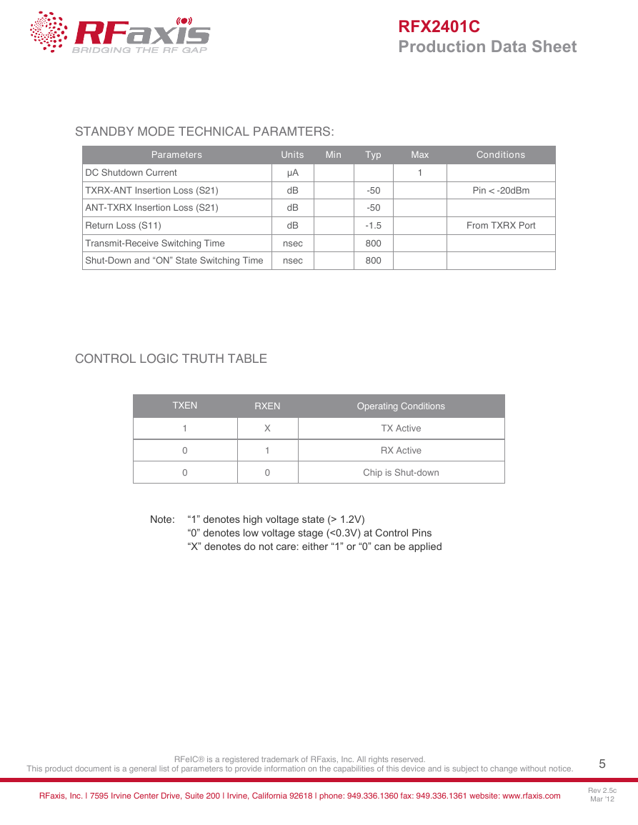
STANDBY MODE TECHNICAL PARAMTERS:
Parameters
Units
Min
Typ
Max
Conditions
DC Shutdown Current
TXRX-ANT Insertion Loss (S21)
ANT-TXRX Insertion Loss (S21)
Return Loss (S11)
μA
dB
dB
dB
Transmit-Receive Switching Time
nsec
Shut-Down and “ON” State Switching Time
nsec
-50
-50
-1.5
800
800
1
Pin < -20dBm
From TXRX Port
CONTROL LOGIC TRUTH TABLE
TXEN
RXEN
1
0
0
X
1
0
Operating Conditions
TX Active
RX Active
Chip is Shut-down
Note:
“1” denotes high voltage state (> 1.2V)
“0” denotes low voltage stage (<0.3V) at Control Pins
“X” denotes do not care: either “1” or “0” can be applied
This product document is a general list of parameters to provide information on the capabilities of this device and is subject to change without notice.
RFeIC® is a registered trademark of RFaxis, Inc. All rights reserved.
RFaxis, Inc. | 7595 Irvine Center Drive, Suite 200 | Irvine, California 92618 | phone: 949.336.1360 fax: 949.336.1361 website: www.rfaxis.com
5
Rev 2.5c
Mar '12
�
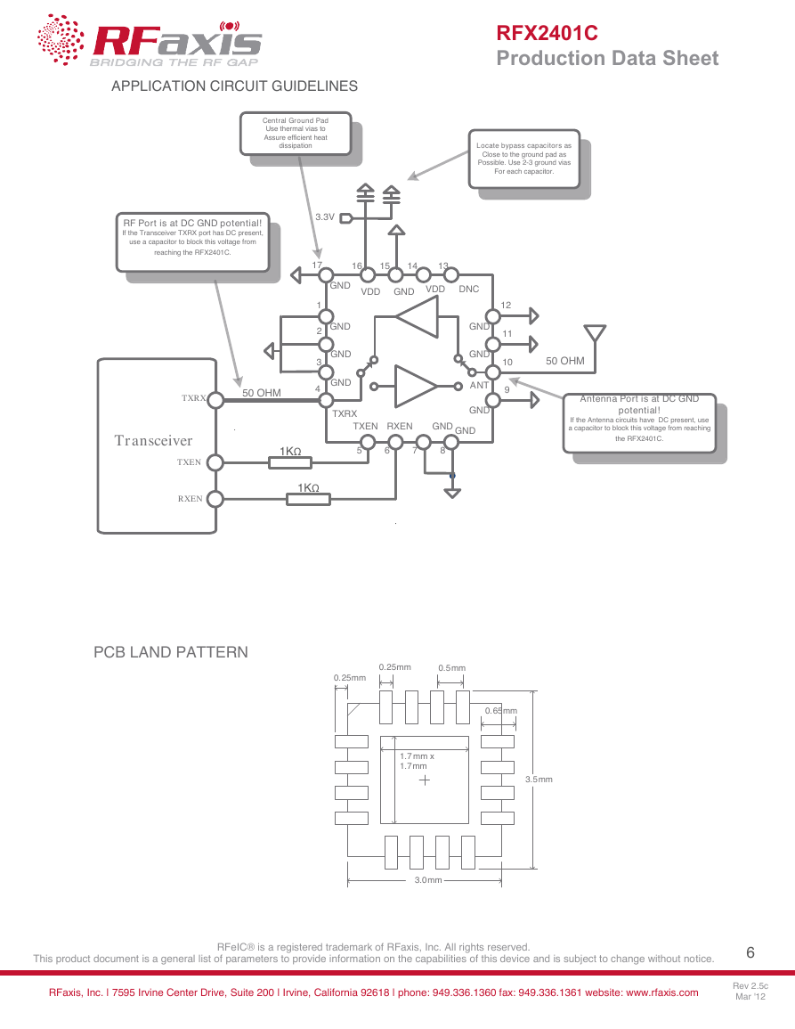
APPLICATION CIRCUIT GUIDELINES
RFX2401C
Production Data Sheet
PCB LAND PATTERN
This product document is a general list of parameters to provide information on the capabilities of this device and is subject to change without notice.
RFeIC® is a registered trademark of RFaxis, Inc. All rights reserved.
RFaxis, Inc. | 7595 Irvine Center Drive, Suite 200 | Irvine, California 92618 | phone: 949.336.1360 fax: 949.336.1361 website: www.rfaxis.com
6
Rev 2.5c
Mar '12
GNDGND12341211109151614135678GND17GNDGNDGNDGNDDNCGNDVDDVDDGNDTXRXGNDANTRXENTXENTransceiverTXRXTXEN50 OHM. Central Ground PadUse thermal vias toAssure efficient heatdissipationRF Port is at DC GND potential!If the Transceiver TXRX port has DC present, use a capacitor to block this voltage from reaching the RFX2401C.Locate bypass capacitors asClose to the ground pad asPossible. Use 2-3 ground viasFor each capacitor.Antenna Port is at DC GND potential!If the Antenna circuits have DC present, use a capacitor to block this voltage from reaching the RFX2401C.50 OHM3.3V1KΩ1KΩRXEN3.5mm3.0mm1.7mm x1.7mm0.65mm0.5mm0.25mm0.25mm�
RFX2401C
Production Data Sheet
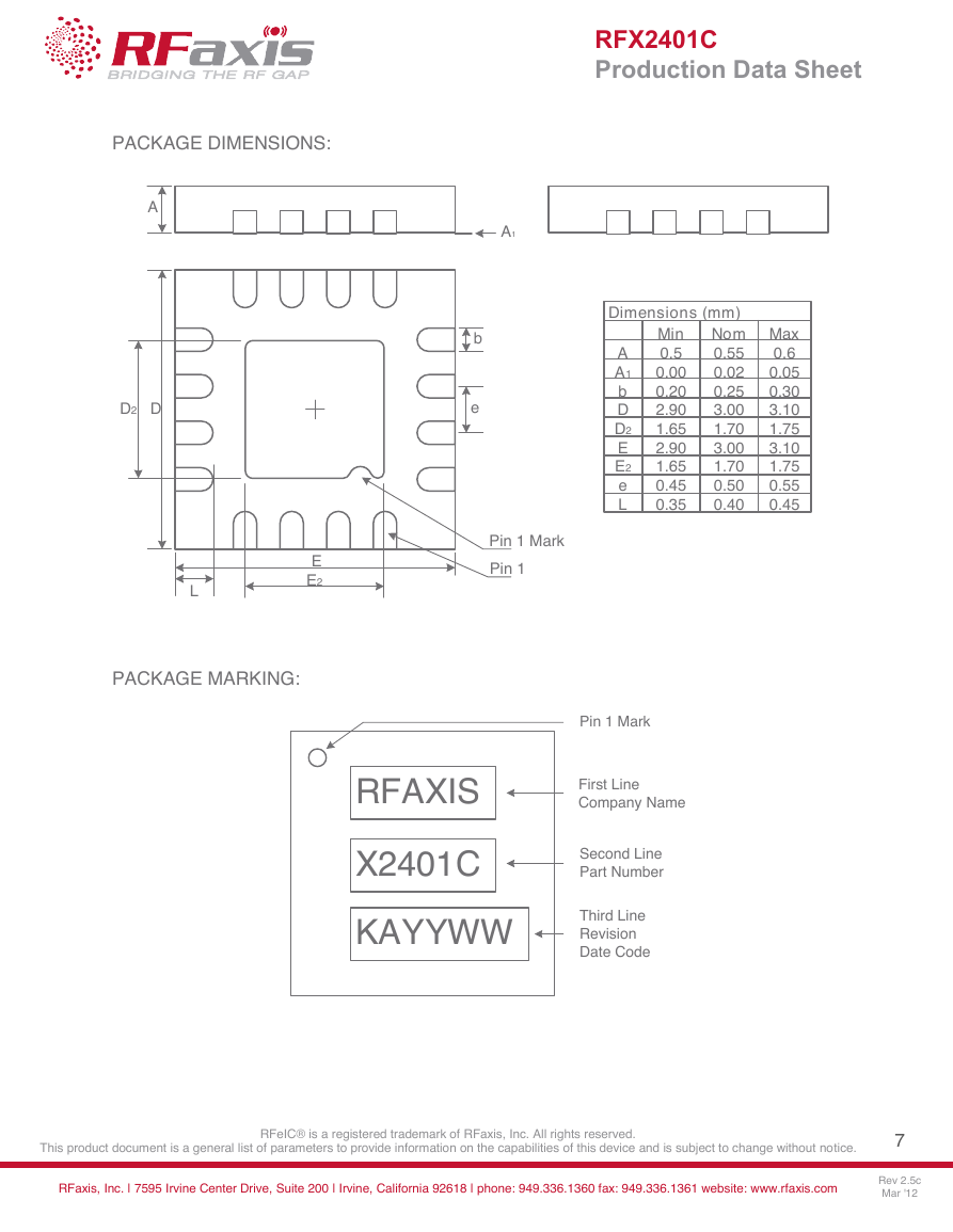
PACKAGE DIMENSIONS:
PACKAGE MARKING:
This product document is a general list of parameters to provide information on the capabilities of this device and is subject to change without notice.
RFeIC® is a registered trademark of RFaxis, Inc. All rights reserved.
RFaxis, Inc. | 7595 Irvine Center Drive, Suite 200 | Irvine, California 92618 | phone: 949.336.1360 fax: 949.336.1361 website: www.rfaxis.com
7
Rev 2.5c
Mar '12
AA1bDED2E2Pin 1 MarkPin 1eAA1bDD2EE2eLMin0.50.000.202.901.652.901.650.450.35Nom0.550.020.253.001.703.001.700.500.40Max0.60.050.303.101.753.101.750.550.45Dimensions (mm)LRFAXISPin 1 MarkSecond LinePart NumberThird LineRevisionDate CodeX2401CKAYYWWFirst LineCompany Name�
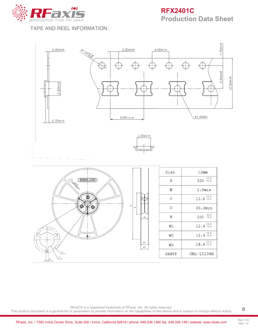
TAPE AND REEL INFORMATION:
RFX2401C
Production Data Sheet
This product document is a general list of parameters to provide information on the capabilities of this device and is subject to change without notice.
RFeIC® is a registered trademark of RFaxis, Inc. All rights reserved.
RFaxis, Inc. | 7595 Irvine Center Drive, Suite 200 | Irvine, California 92618 | phone: 949.336.1360 fax: 949.336.1361 website: www.rfaxis.com
8
Rev 2.5c
Mar '12
�
