The Future of Analog IC Technology
MP2303
3A, 28V, 340KHz Synchronous Rectified
Step-Down Converter
transient
DESCRIPTION
The MP2303 is a monolithic synchronous buck
regulator. The device
integrates power
MOSFETS that provide 3A continuous load
current over a wide operating input voltage of
4.75V to 28V. Current mode control provides
fast
response and cycle-by-cycle
current limit.
An adjustable soft-start prevents inrush current
at turn-on. In shutdown mode, the supply
current drops to 1μA.
This device, available in 8-pin SOIC and 3x3
10-pin QFN packages, provides a very compact
system solution with minimal
reliance on
external components.
EVALUATION BOARD REFERENCE
Dimensions
Board Number
EV2303DN-00A
2.0”X x 1.5”Y x 0.5”Z
FEATURES
• 3A Output Current
• Wide 4.75V to 28V Operating Input Range
•
Integrated Power MOSFET Switches
• Output Adjustable from 0.8V to 25V
• Up to 95% Efficiency
• Programmable Soft-Start
• Stable with Low ESR Ceramic Output Capacitors
• Fixed 340KHz Frequency
• Cycle-by-Cycle Over Current Protection
•
• Thermally Enhanced 8-Pin SOIC and
Input Under Voltage Lockout
3x3 QFN10 Packages
APPLICATIONS
• Distributed Power Systems
• Pre-Regulator for Linear Regulators
• Notebook Computers
“MPS” and “The Future of Analog IC Technology” are Registered Trademarks of
Monolithic Power Systems, Inc.
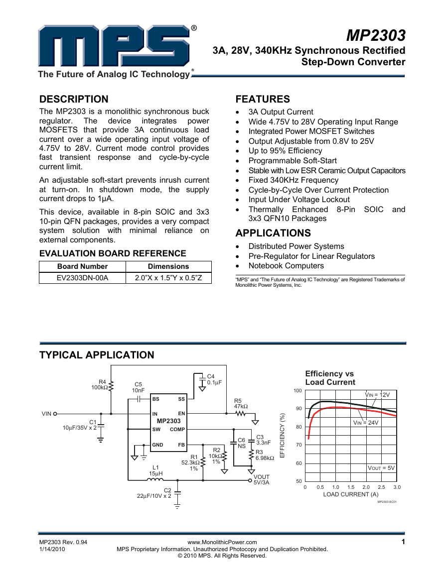
TYPICAL APPLICATION
R4
100kΩ
C5
10nF
VIN
C1
10μF/35V x 2
MP2303 Rev. 0.94
1/14/2010
C4
0.1μF
R2
10kΩ
1%
R5
47kΩ
C6
NS
C3
3.3nF
R3
6.98kΩ
VOUT
5V/3A
)
%
(
I
Y
C
N
E
C
F
F
E
I
100
90
80
70
60
50
Efficiency vs
Load Current
VIN = 12V
VIN = 24V
VOUT = 5V
0
0.5
1.0
1.5
2.0
2.5
3.0
LOAD CURRENT (A)
MP2303-EC01
BS
SS
EN
IN
MP2303
SW
COMP
GND
FB
R1
52.3kΩ
1%
L1
15μH
C2
22μF/10V x 2
MPS Proprietary Information. Unauthorized Photocopy and Duplication Prohibited.
www.MonolithicPower.com
© 2010 MPS. All Rights Reserved.
1
�
MP2303 – 3A, 28V, 340KHz SYNCHRONOUS RECTIFIED, STEP-DOWN CONVERTER
ORDERING INFORMATION
Part Number
MP2303DN*
MP2303DQ**
Package
SOIC8E (Exposed Pad)
QFN10 (3mm x 3mm)
* For Tape & Reel, add suffix –Z (e.g. MP2303DN–Z);
K2
Top Marking
MP2303DN
Temperature
–40°C to +85°C
MP2303DQ
For RoHS compliant packaging, add suffix –LF (e.g. MP2303DN–LF–Z)
** For Tape & Reel, add suffix –Z (e.g. MP2303DQ–Z);
For RoHS compliant packaging, add suffix –LF (e.g. MP2303DQ–LF–Z)
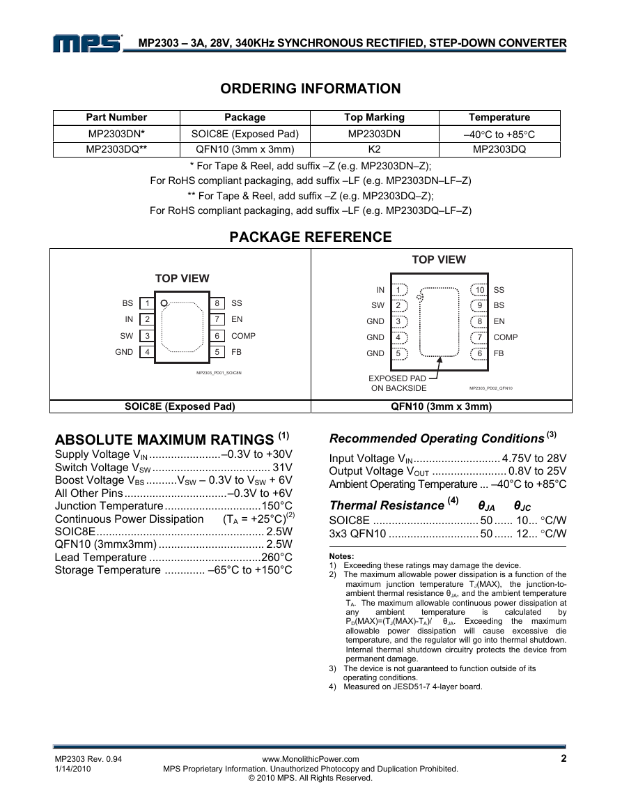
PACKAGE REFERENCE
TOP VIEW
TOP VIEW
BS
IN
SW
GND
1
2
3
4
8
7
6
5
SS
EN
COMP
FB
MP2303_PD01_SOIC8N
SOIC8E (Exposed Pad)
ABSOLUTE MAXIMUM RATINGS (1)
Supply Voltage VIN .......................–0.3V to +30V
Switch Voltage VSW ...................................... 31V
Boost Voltage VBS ..........VSW – 0.3V to VSW + 6V
All Other Pins.................................–0.3V to +6V
Junction Temperature...............................150°C
Continuous Power Dissipation (TA = +25°C)(2)
SOIC8E...................................................... 2.5W
QFN10 (3mmx3mm) .................................. 2.5W
Lead Temperature ....................................260°C
Storage Temperature ............. –65°C to +150°C
IN
SW
GND
GND
GND
1
2
3
4
5
10
9
8
7
6
SS
BS
EN
COMP
FB
EXPOSED PAD
ON BACKSIDE
MP2303_PD02_QFN10
QFN10 (3mm x 3mm)
Recommended Operating Conditions (3)
Input Voltage VIN............................ 4.75V to 28V
Output Voltage VOUT ........................ 0.8V to 25V
Ambient Operating Temperature ... –40°C to +85°C
Thermal Resistance (4)
SOIC8E .................................. 50...... 10... °C/W
3x3 QFN10 ............................. 50...... 12... °C/W
θJC
θJA
Notes:
1) Exceeding these ratings may damage the device.
2) The maximum allowable power dissipation is a function of the
maximum junction temperature TJ(MAX), the junction-to-
ambient thermal resistance θJA, and the ambient temperature
TA. The maximum allowable continuous power dissipation at
by
any
PD(MAX)=(TJ(MAX)-TA)/ θJA. Exceeding
the maximum
allowable power dissipation will cause excessive die
temperature, and the regulator will go into thermal shutdown.
Internal thermal shutdown circuitry protects the device from
permanent damage.
temperature
calculated
ambient
is
3) The device is not guaranteed to function outside of its
operating conditions.
4) Measured on JESD51-7 4-layer board.
MP2303 Rev. 0.94
1/14/2010
MPS Proprietary Information. Unauthorized Photocopy and Duplication Prohibited.
www.MonolithicPower.com
© 2010 MPS. All Rights Reserved.
2
�
MP2303 – 3A, 28V, 340KHz SYNCHRONOUS RECTIFIED, STEP-DOWN CONVERTER
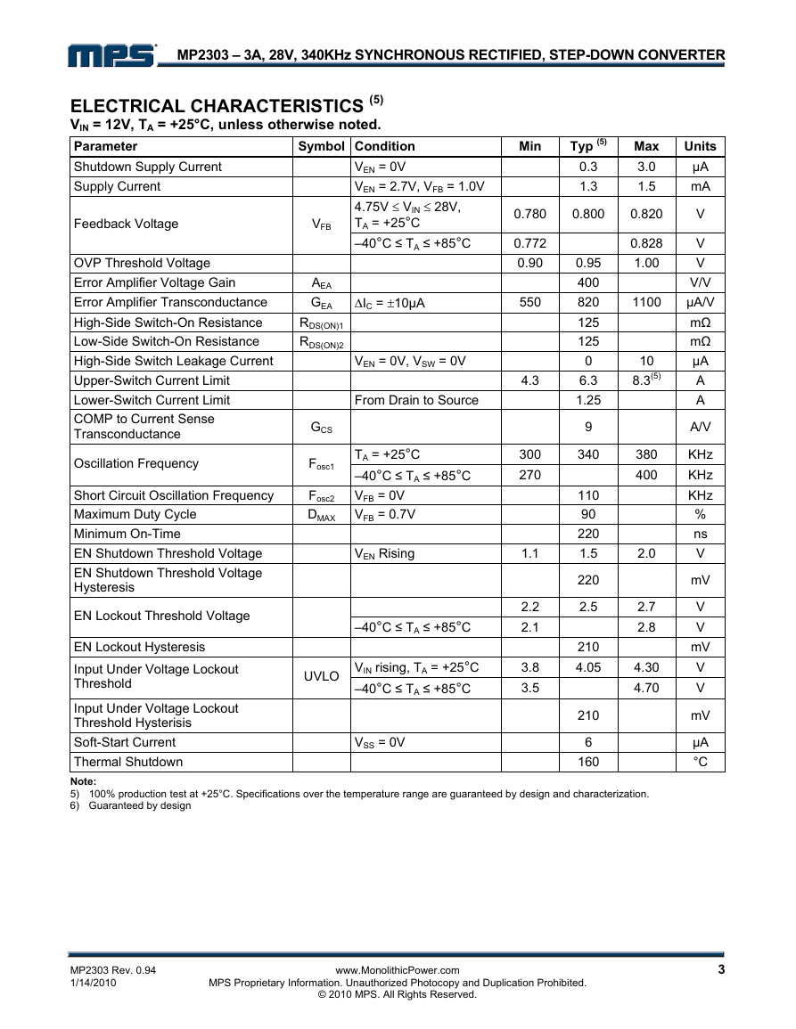
ELECTRICAL CHARACTERISTICS (5)
VIN = 12V, TA = +25°C, unless otherwise noted.
Parameter
Shutdown Supply Current
Supply Current
Symbol Condition
Feedback Voltage
OVP Threshold Voltage
Error Amplifier Voltage Gain
Error Amplifier Transconductance
High-Side Switch-On Resistance
Low-Side Switch-On Resistance
High-Side Switch Leakage Current
Upper-Switch Current Limit
Lower-Switch Current Limit
COMP to Current Sense
Transconductance
Oscillation Frequency
Short Circuit Oscillation Frequency
Maximum Duty Cycle
Minimum On-Time
EN Shutdown Threshold Voltage
EN Shutdown Threshold Voltage
Hysteresis
EN Lockout Threshold Voltage
Min
Typ (5)
0.3
1.3
Max
3.0
1.5
Units
μA
mA
0.780
0.800
0.820
V
0.772
0.90
550
4.3
300
270
1.1
2.2
2.1
0.95
400
820
125
125
0
6.3
1.25
9
340
110
90
220
1.5
220
2.5
0.828
1.00
1100
10
8.3(5)
380
400
2.0
2.7
2.8
VEN = 0V
VEN = 2.7V, VFB = 1.0V
4.75V ≤ VIN ≤ 28V,
TA = +25°C
–40°C ≤ TA ≤ +85°C
ΔIC = ±10μA
VEN = 0V, VSW = 0V
From Drain to Source
VFB
AEA
GEA
RDS(ON)1
RDS(ON)2
GCS
Fosc1
TA = +25°C
–40°C ≤ TA ≤ +85°C
Fosc2 VFB = 0V
DMAX VFB = 0.7V
VEN Rising
–40°C ≤ TA ≤ +85°C
VIN rising, TA = +25°C
–40°C ≤ TA ≤ +85°C
V
V
V/V
μA/V
mΩ
mΩ
μA
A
A
A/V
KHz
KHz
KHz
%
ns
V
mV
V
V
mV
V
V
mV
μA
°C
3
UVLO
EN Lockout Hysteresis
Input Under Voltage Lockout
Threshold
Input Under Voltage Lockout
Threshold Hysterisis
Soft-Start Current
Thermal Shutdown
Note:
5) 100% production test at +25°C. Specifications over the temperature range are guaranteed by design and characterization.
6) Guaranteed by design
VSS = 0V
210
4.05
6
160
3.8
3.5
210
4.30
4.70
MP2303 Rev. 0.94
1/14/2010
MPS Proprietary Information. Unauthorized Photocopy and Duplication Prohibited.
www.MonolithicPower.com
© 2010 MPS. All Rights Reserved.
�
MP2303 – 3A, 28V, 340KHz SYNCHRONOUS RECTIFIED, STEP-DOWN CONVERTER
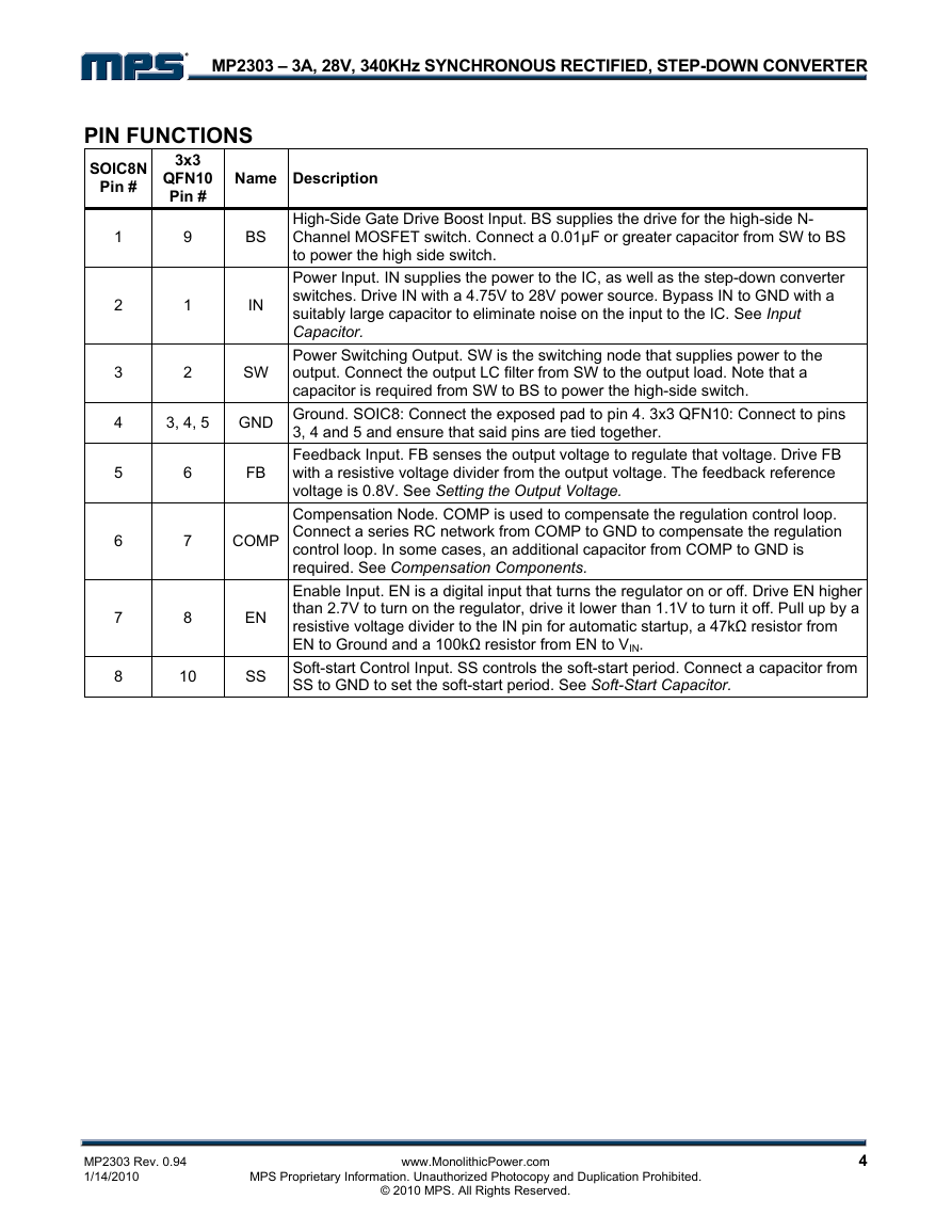
PIN FUNCTIONS
SOIC8N
Pin #
3x3
QFN10
Pin #
Name Description
1
2
3
4
5
6
7
8
9
1
2
3, 4, 5
6
7
8
10
MP2303 Rev. 0.94
1/14/2010
BS
IN
SW
High-Side Gate Drive Boost Input. BS supplies the drive for the high-side N-
Channel MOSFET switch. Connect a 0.01μF or greater capacitor from SW to BS
to power the high side switch.
Power Input. IN supplies the power to the IC, as well as the step-down converter
switches. Drive IN with a 4.75V to 28V power source. Bypass IN to GND with a
suitably large capacitor to eliminate noise on the input to the IC. See Input
Capacitor.
Power Switching Output. SW is the switching node that supplies power to the
output. Connect the output LC filter from SW to the output load. Note that a
capacitor is required from SW to BS to power the high-side switch.
FB
COMP
GND Ground. SOIC8: Connect the exposed pad to pin 4. 3x3 QFN10: Connect to pins
3, 4 and 5 and ensure that said pins are tied together.
Feedback Input. FB senses the output voltage to regulate that voltage. Drive FB
with a resistive voltage divider from the output voltage. The feedback reference
voltage is 0.8V. See Setting the Output Voltage.
Compensation Node. COMP is used to compensate the regulation control loop.
Connect a series RC network from COMP to GND to compensate the regulation
control loop. In some cases, an additional capacitor from COMP to GND is
required. See Compensation Components.
Enable Input. EN is a digital input that turns the regulator on or off. Drive EN higher
than 2.7V to turn on the regulator, drive it lower than 1.1V to turn it off. Pull up by a
resistive voltage divider to the IN pin for automatic startup, a 47kΩ resistor from
EN to Ground and a 100kΩ resistor from EN to VIN.
Soft-start Control Input. SS controls the soft-start period. Connect a capacitor from
SS to GND to set the soft-start period. See Soft-Start Capacitor.
EN
SS
MPS Proprietary Information. Unauthorized Photocopy and Duplication Prohibited.
www.MonolithicPower.com
© 2010 MPS. All Rights Reserved.
4
�
MP2303 – 3A, 28V, 340KHz SYNCHRONOUS RECTIFIED, STEP-DOWN CONVERTER
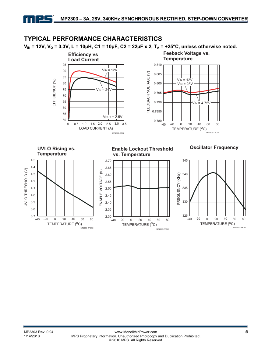
TYPICAL PERFORMANCE CHARACTERISTICS
VIN = 12V, VO = 3.3V, L = 10µH, C1 = 10µF, C2 = 22µF x 2, TA = +25°C, unless otherwise noted.
Efficiency vs
Load Current
95
90
85
80
75
70
65
60
55
50
0
0.5
VIN = 12V
VIN = 24V
VOUT = 2.5V
1.0
1.5 2.0
2.5
LOAD CURRENT (A)
3.0
3.5
)
%
(
I
Y
C
N
E
C
F
F
E
I
Feeback Voltage vs.
Temperature
)
V
(
E
G
A
T
L
O
V
K
C
A
B
D
E
E
F
0.810
0.805
0.800
0.795
0.790
0.7850
0.780
-40
VIN = 12V
VIN = 28V
VIN = 4.75V
0
-20
TEMPERATURE (oC)
20
40
60
80
MP2303-EC02
MP2303-TPC01
UVLO Rising vs.
Temperature
Enable Lockout Threshold
vs. Temperature
Oscillator Frequency
)
V
(
D
L
O
H
S
E
R
H
T
O
L
V
U
4.5
4.4
4.3
4.2
4.1
4.0
3.9
3.8
3.7
-40
2.70
2.65
2.60
2.55
2.50
2.45
2.40
2.35
)
V
(
E
G
A
T
L
O
V
E
L
B
A
N
E
-20
0
20
60
TEMPERATURE (oC)
40
80
2.30
-40
0
-20
TEMPERATURE (oC)
20
40
345
340
335
330
)
z
H
K
(
Y
C
N
E
U
Q
E
R
F
60
80
325
-40
-20
0
20
60
TEMPERATURE (oC)
40
80
MP2303-TPC02
MP2303-TPC03
MP2303 Rev. 0.94
1/14/2010
MPS Proprietary Information. Unauthorized Photocopy and Duplication Prohibited.
www.MonolithicPower.com
© 2010 MPS. All Rights Reserved.
MP2303-TPC04
5
�
MP2303 – 3A, 28V, 340KHz SYNCHRONOUS RECTIFIED, STEP-DOWN CONVERTER
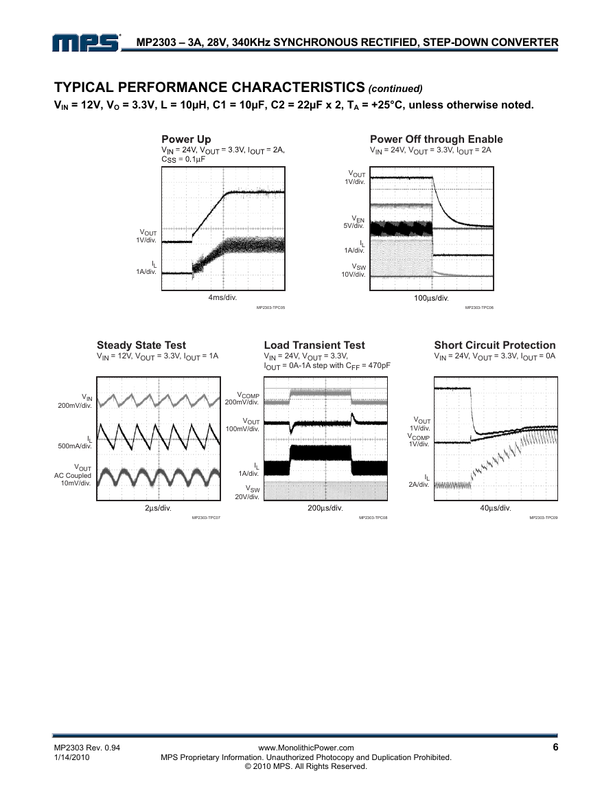
TYPICAL PERFORMANCE CHARACTERISTICS (continued)
VIN = 12V, VO = 3.3V, L = 10µH, C1 = 10µF, C2 = 22µF x 2, TA = +25°C, unless otherwise noted.
Power Off through Enable
VIN = 24V, VOUT = 3.3V, IOUT = 2A
VOUT
1V/div.
IL
1A/div.
VOUT
1V/div.
VEN
5V/div.
IL
1A/div.
VSW
10V/div.
4ms/div.
MP2303-TPC05
MP2303-TPC06
Steady State Test
VIN = 12V, VOUT = 3.3V, IOUT = 1A
Load Transient Test
VIN = 24V, VOUT = 3.3V,
IOUT = 0A-1A step with CFF = 470pF
Short Circuit Protection
VIN = 24V, VOUT = 3.3V, IOUT = 0A
VIN
200mV/div.
IL
500mA/div.
VOUT
AC Coupled
10mV/div.
VCOMP
200mV/div.
VOUT
100mV/div.
IL
1A/div.
VSW
20V/div.
VOUT
1V/div.
VCOMP
1V/div.
IL
2A/div.
MP2303-TPC07
MP2303-TPC08
MP2303-TPC09
MP2303 Rev. 0.94
1/14/2010
MPS Proprietary Information. Unauthorized Photocopy and Duplication Prohibited.
www.MonolithicPower.com
© 2010 MPS. All Rights Reserved.
6
�
MP2303 – 3A, 28V, 340KHz SYNCHRONOUS RECTIFIED, STEP-DOWN CONVERTER
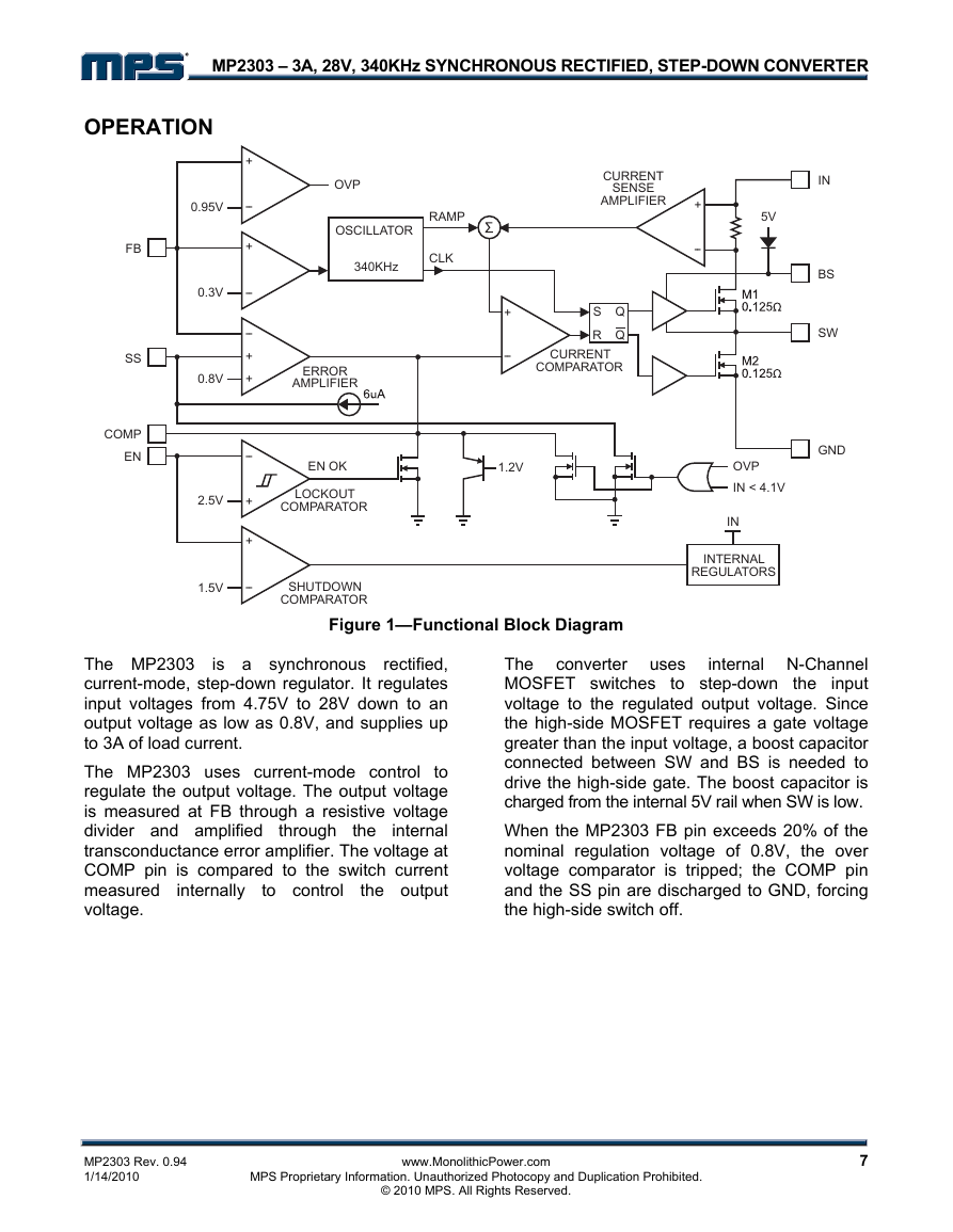
OPERATION
FB
SS
COMP
EN
+
--
+
--
--
+
+
--
+
+
--
0.95V
0.3V
0.8V
2.5V
1.5V
OVP
OSCILLATOR
340KHz
RAMP
CLK
ERROR
AMPLIFIER
EN OK
LOCKOUT
COMPARATOR
SHUTDOWN
COMPARATOR
CURRENT
SENSE
AMPLIFIER
+
--
S
R
Q
Q
CURRENT
COMPARATOR
1.2V
+
--
5V
OVP
IN < 4.1V
IN
INTERNAL
REGULATORS
IN
BS
SW
GND
Figure 1—Functional Block Diagram
is a synchronous
rectified,
The MP2303
current-mode, step-down regulator. It regulates
input voltages from 4.75V to 28V down to an
output voltage as low as 0.8V, and supplies up
to 3A of load current.
The MP2303 uses current-mode control to
regulate the output voltage. The output voltage
is measured at FB through a resistive voltage
divider and amplified
internal
transconductance error amplifier. The voltage at
COMP pin is compared to the switch current
measured
the output
voltage.
to control
internally
through
the
the
to step-down
converter uses
internal N-Channel
The
MOSFET switches
input
voltage to the regulated output voltage. Since
the high-side MOSFET requires a gate voltage
greater than the input voltage, a boost capacitor
connected between SW and BS is needed to
drive the high-side gate. The boost capacitor is
charged from the internal 5V rail when SW is low.
When the MP2303 FB pin exceeds 20% of the
nominal regulation voltage of 0.8V, the over
voltage comparator is tripped; the COMP pin
and the SS pin are discharged to GND, forcing
the high-side switch off.
MP2303 Rev. 0.94
1/14/2010
MPS Proprietary Information. Unauthorized Photocopy and Duplication Prohibited.
www.MonolithicPower.com
© 2010 MPS. All Rights Reserved.
7
�
MP2303 – 3A, 28V, 340KHz SYNCHRONOUS RECTIFIED, STEP-DOWN CONVERTER
APPLICATIONS INFORMATION
COMPONENT SELECTION
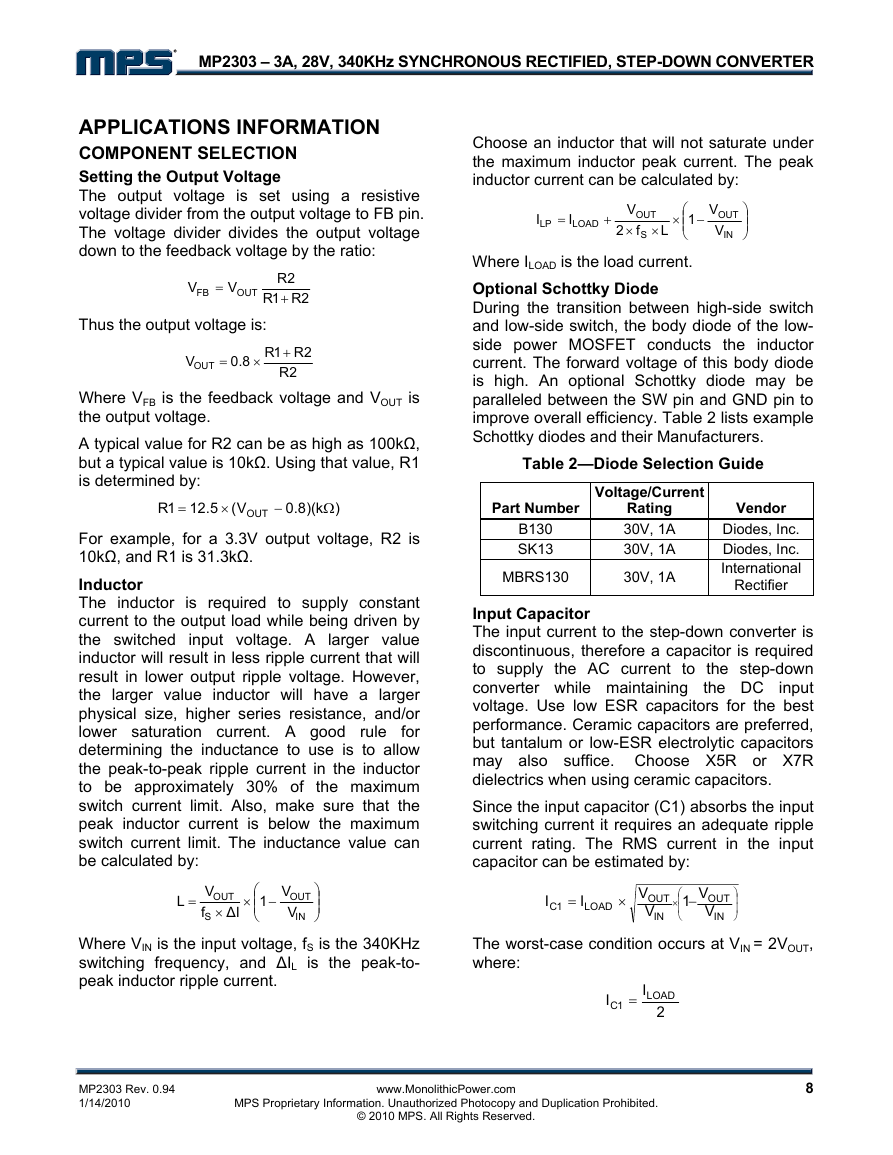
Setting the Output Voltage
The output voltage is set using a resistive
voltage divider from the output voltage to FB pin.
The voltage divider divides the output voltage
down to the feedback voltage by the ratio:
V
FB
=
V
OUT
2R
+
2R1R
Thus the output voltage is:
VOUT
=
2R1R8.0
×
+
2R
Where VFB is the feedback voltage and VOUT is
the output voltage.
A typical value for R2 can be as high as 100kΩ,
but a typical value is 10kΩ. Using that value, R1
is determined by:
1R
=
V(5.12
×
OUT
−
)k)(8.0
Ω
For example, for a 3.3V output voltage, R2 is
10kΩ, and R1 is 31.3kΩ.
Inductor
The inductor is required to supply constant
current to the output load while being driven by
the switched input voltage. A larger value
inductor will result in less ripple current that will
result in lower output ripple voltage. However,
the larger value inductor will have a larger
physical size, higher series resistance, and/or
lower saturation current. A good rule
for
determining the inductance to use is to allow
the peak-to-peak ripple current in the inductor
to be approximately 30% of the maximum
switch current limit. Also, make sure that the
peak inductor current is below the maximum
switch current limit. The inductance value can
be calculated by:
L
=
V
OUT
ΔI
f
×
S
×
⎛
⎜⎜
⎝
V1
OUT
−
V
IN
⎞
⎟⎟
⎠
Where VIN is the input voltage, fS is the 340KHz
switching frequency, and ΔIL is the peak-to-
peak inductor ripple current.
Choose an inductor that will not saturate under
the maximum inductor peak current. The peak
inductor current can be calculated by:
×
L
S
+
⎞
⎟⎟
⎠
=
I
1
−
I
LP
LOAD
V
OUT
V
IN
V
OUT
f2
×
×
⎛
⎜⎜
⎝
Where ILOAD is the load current.
Optional Schottky Diode
During the transition between high-side switch
and low-side switch, the body diode of the low-
side power MOSFET conducts the inductor
current. The forward voltage of this body diode
is high. An optional Schottky diode may be
paralleled between the SW pin and GND pin to
improve overall efficiency. Table 2 lists example
Schottky diodes and their Manufacturers.
Table 2—Diode Selection Guide
Part Number
B130
SK13
MBRS130
Voltage/Current
Rating
30V, 1A
30V, 1A
30V, 1A
Vendor
Diodes, Inc.
Diodes, Inc.
International
Rectifier
the DC
Input Capacitor
The input current to the step-down converter is
discontinuous, therefore a capacitor is required
to supply the AC current to the step-down
converter while maintaining
input
voltage. Use low ESR capacitors for the best
performance. Ceramic capacitors are preferred,
but tantalum or low-ESR electrolytic capacitors
may also suffice. Choose X5R or X7R
dielectrics when using ceramic capacitors.
Since the input capacitor (C1) absorbs the input
switching current it requires an adequate ripple
current rating. The RMS current in the input
capacitor can be estimated by:
I
1C
=
I
LOAD
×
V
OUT
V
IN
V1
⎛
OUT
× −
⎜
V
⎜
IN
⎝
⎞
⎟
⎟
⎠
The worst-case condition occurs at VIN = 2VOUT,
where:
I
1C =
I
LOAD
2
MP2303 Rev. 0.94
1/14/2010
MPS Proprietary Information. Unauthorized Photocopy and Duplication Prohibited.
www.MonolithicPower.com
© 2010 MPS. All Rights Reserved.
8
�
