logo资料库

MPU-6000 and MPU-6050 Register Map and Descriptions(MPU6050资料).pdf

第1页 / 共47页
第2页 / 共47页
第3页 / 共47页
第4页 / 共47页
第5页 / 共47页
第6页 / 共47页
第7页 / 共47页
第8页 / 共47页
资料共47页,剩余部分请下载后查看
Revision History
2 Purpose and Scope
3 Register Map
4 Register Descriptions
4.1 Registers 13 to 16 – Self Test Registers
1. Gyroscope Hardware Self-Test: Relative Method
2. Accelerometer Hardware Self-Test: Relative Method
4.2 Register 25 – Sample Rate Divider
4.3 Register 26 – Configuration
4.4 Register 27 – Gyroscope Configuration
4.5 Register 28 – Accelerometer Configuration
4.6 Register 31 – Motion Detection Threshold
4.7 Register 35 – FIFO Enable
4.8 Register 36 – I2C Master Control
4.9 Registers 37 to 39 – I2C Slave 0 Control
4.10 Registers 40 to 42 – I2C Slave 1 Control
4.11 Registers 43 to 45 – I2C Slave 2 Control
4.12 Registers 46 to 48 – I2C Slave 3 Control
4.13 Registers 49 to 53 – I2C Slave 4 Control
4.14 Register 54 – I2C Master Status
4.15 Register 55 – INT Pin / Bypass Enable Configuration
4.16 Register 56 – Interrupt Enable
4.17 Register 58 – Interrupt Status
4.18 Registers 59 to 64 – Accelerometer Measurements
4.19 Registers 65 and 66 – Temperature Measurement
4.20 Registers 67 to 72 – Gyroscope Measurements
4.21 Registers 73 to 96 – External Sensor Data
4.22 Register 99 – I2C Slave 0 Data Out
4.23 Register 100 – I2C Slave 1 Data Out
4.24 Register 101 – I2C Slave 2 Data Out
4.25 Register 102 – I2C Slave 3 Data Out
4.26 Register 103 – I2C Master Delay Control
4.27 Register 104 – Signal Path Reset
4.28 Register 105 – Motion Detection Control
4.29 Register 106 – User Control
4.30 Register 107 – Power Management 1
4.31 Register 108 – Power Management 2
4.32 Register 114 and 115 – FIFO Count Registers
4.33 Register 116 – FIFO Read Write
4.34 Register 117 – Who Am I
InvenSense Inc. 1197 Borregas Ave, Sunnyvale, CA 94089 U.S.A. Tel: +1 (408) 988-7339 Fax: +1 (408) 988-8104 Website: www.invensense.com Document Number: RM-MPU-6000A-00 Revision: 4.0 Release Date: 03/09/2012 MPU-6000 and MPU-6050 Register Map and Descriptions Revision 4.0 CONFIDENTIAL & PROPRIETARY 1 of 47
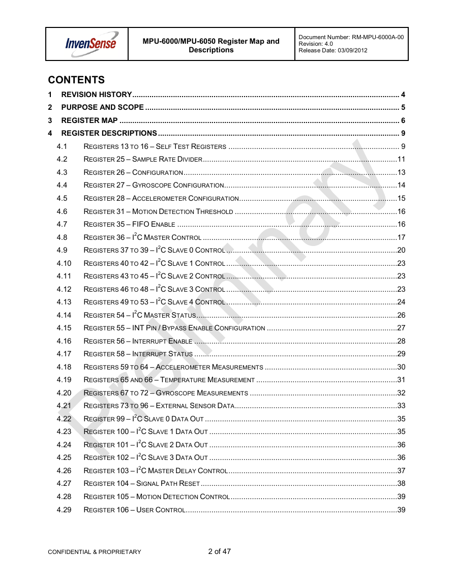
MPU-6000/MPU-6050 Register Map and Descriptions Document Number: RM-MPU-6000A-00 Revision: 4.0 Release Date: 03/09/2012 CONTENTS 1 REVISION HISTORY ............................................................................................................................. 4 2 PURPOSE AND SCOPE ....................................................................................................................... 5 3 REGISTER MAP ................................................................................................................................... 6 4 REGISTER DESCRIPTIONS ................................................................................................................. 9 REGISTERS 13 TO 16 – SELF TEST REGISTERS ................................................................................ 9 4.1 REGISTER 25 – SAMPLE RATE DIVIDER ...........................................................................................11 4.2 REGISTER 26 – CONFIGURATION ....................................................................................................13 4.3 REGISTER 27 – GYROSCOPE CONFIGURATION.................................................................................14 4.4 REGISTER 28 – ACCELEROMETER CONFIGURATION..........................................................................15 4.5 REGISTER 31 – MOTION DETECTION THRESHOLD ............................................................................16 4.6 REGISTER 35 – FIFO ENABLE .......................................................................................................16 4.7 REGISTER 36 – I2C MASTER CONTROL ...........................................................................................17 4.8 REGISTERS 37 TO 39 – I2C SLAVE 0 CONTROL ................................................................................20 4.9 4.10 REGISTERS 40 TO 42 – I2C SLAVE 1 CONTROL ................................................................................23 4.11 REGISTERS 43 TO 45 – I2C SLAVE 2 CONTROL ................................................................................23 4.12 REGISTERS 46 TO 48 – I2C SLAVE 3 CONTROL ................................................................................23 4.13 REGISTERS 49 TO 53 – I2C SLAVE 4 CONTROL ................................................................................24 4.14 REGISTER 54 – I2C MASTER STATUS ..............................................................................................26 4.15 REGISTER 55 – INT PIN / BYPASS ENABLE CONFIGURATION .............................................................27 4.16 REGISTER 56 – INTERRUPT ENABLE ...............................................................................................28 4.17 REGISTER 58 – INTERRUPT STATUS ...............................................................................................29 4.18 REGISTERS 59 TO 64 – ACCELEROMETER MEASUREMENTS ..............................................................30 4.19 REGISTERS 65 AND 66 – TEMPERATURE MEASUREMENT ..................................................................31 4.20 REGISTERS 67 TO 72 – GYROSCOPE MEASUREMENTS .....................................................................32 4.21 REGISTERS 73 TO 96 – EXTERNAL SENSOR DATA ............................................................................33 4.22 REGISTER 99 – I2C SLAVE 0 DATA OUT ..........................................................................................35 4.23 REGISTER 100 – I2C SLAVE 1 DATA OUT ........................................................................................35 4.24 REGISTER 101 – I2C SLAVE 2 DATA OUT ........................................................................................36 4.25 REGISTER 102 – I2C SLAVE 3 DATA OUT ........................................................................................36 4.26 REGISTER 103 – I2C MASTER DELAY CONTROL ...............................................................................37 4.27 REGISTER 104 – SIGNAL PATH RESET ............................................................................................38 4.28 REGISTER 105 – MOTION DETECTION CONTROL ..............................................................................39 4.29 REGISTER 106 – USER CONTROL...................................................................................................39 CONFIDENTIAL & PROPRIETARY 2 of 47
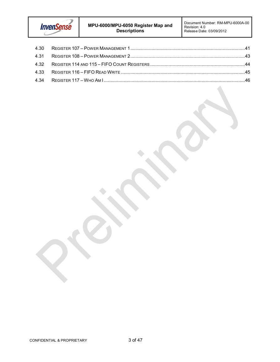
MPU-6000/MPU-6050 Register Map and Descriptions Document Number: RM-MPU-6000A-00 Revision: 4.0 Release Date: 03/09/2012 4.30 REGISTER 107 – POWER MANAGEMENT 1 .......................................................................................41 4.31 REGISTER 108 – POWER MANAGEMENT 2 .......................................................................................43 4.32 REGISTER 114 AND 115 – FIFO COUNT REGISTERS ........................................................................44 4.33 REGISTER 116 – FIFO READ WRITE ..............................................................................................45 4.34 REGISTER 117 – WHO AM I ...........................................................................................................46 CONFIDENTIAL & PROPRIETARY 3 of 47
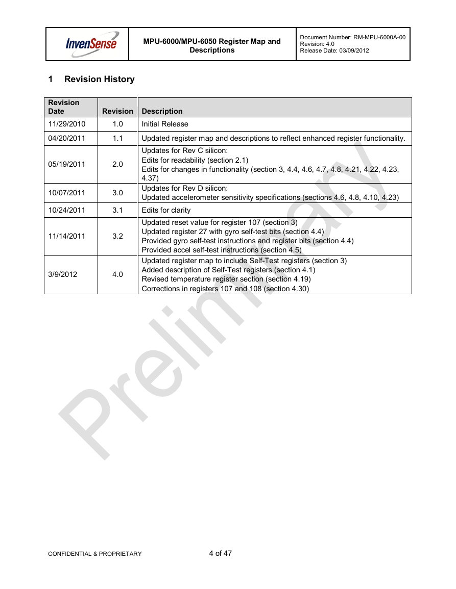
MPU-6000/MPU-6050 Register Map and Descriptions Document Number: RM-MPU-6000A-00 Revision: 4.0 Release Date: 03/09/2012 1 Revision History Revision Date 11/29/2010 04/20/2011 1.0 1.1 Revision Description Initial Release Updated register map and descriptions to reflect enhanced register functionality. Updates for Rev C silicon: Edits for readability (section 2.1) Edits for changes in functionality (section 3, 4.4, 4.6, 4.7, 4.8, 4.21, 4.22, 4.23, 4.37) Updates for Rev D silicon: Updated accelerometer sensitivity specifications (sections 4.6, 4.8, 4.10, 4.23) Edits for clarity Updated reset value for register 107 (section 3) Updated register 27 with gyro self-test bits (section 4.4) Provided gyro self-test instructions and register bits (section 4.4) Provided accel self-test instructions (section 4.5) Updated register map to include Self-Test registers (section 3) Added description of Self-Test registers (section 4.1) Revised temperature register section (section 4.19) Corrections in registers 107 and 108 (section 4.30) 05/19/2011 10/07/2011 10/24/2011 11/14/2011 2.0 3.0 3.1 3.2 3/9/2012 4.0 CONFIDENTIAL & PROPRIETARY 4 of 47
MPU-6000/MPU-6050 Register Map and Descriptions Document Number: RM-MPU-6000A-00 Revision: 4.0 Release Date: 03/09/2012 2 Purpose and Scope This document provides preliminary information regarding the register map and descriptions for the Motion Processing Units™ MPU-6000™ and MPU-6050™, collectively called the MPU-60X0™ or MPU™. The MPU devices provide the world’s first integrated 6-axis motion processor solution that eliminates the package-level gyroscope and accelerometer cross-axis misalignment associated with discrete solutions. The devices combine a 3-axis gyroscope and a 3-axis accelerometer on the same silicon die together with an onboard Digital Motion Processor™ (DMP™) capable of processing complex 9-axis sensor fusion algorithms using the field-proven and proprietary MotionFusion™ engine. The MPU-6000 and MPU-6050’s integrated 9-axis MotionFusion algorithms access external magnetometers or other sensors through an auxiliary master I2C bus, allowing the devices to gather a full set of sensor data without intervention from the system processor. The devices are offered in the same 4x4x0.9 mm QFN footprint and pinout as the current MPU-3000™ family of integrated 3-axis gyroscopes, providing a simple upgrade path and facilitating placement on already space constrained circuit boards. For precision tracking of both fast and slow motions, the MPU-60X0 features a user-programmable gyroscope full-scale range of ±250, ±500, ±1000, and ±2000°/sec (dps). The parts also have a user- programmable accelerometer full-scale range of ±2g, ±4g, ±8g, and ±16g. The MPU-6000 family is comprised of two parts, the MPU-6000 and MPU-6050. These parts are identical to each other with two exceptions. The MPU-6050 supports I2C communications at up to 400kHz and has a VLOGIC pin that defines its interface voltage levels; the MPU-6000 supports SPI at up to 20MHz in addition to I2C, and has a single supply pin, VDD, which is both the device’s logic reference supply and the analog supply for the part. For more detailed information for the MPU-60X0 devices, please refer to the “MPU-6000 and MPU-6050 Product Specification”. CONFIDENTIAL & PROPRIETARY 5 of 47
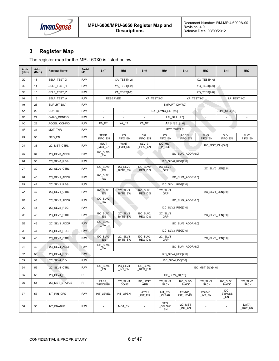
MPU-6000/MPU-6050 Register Map and Descriptions Document Number: RM-MPU-6000A-00 Revision: 4.0 Release Date: 03/09/2012 3 Register Map The register map for the MPU-60X0 is listed below. Addr (Hex) Addr (Dec.) Register Name Serial I/F Bit7 Bit6 Bit5 Bit4 Bit3 Bit2 Bit1 Bit0 SELF_TEST_X SELF_TEST_Y SELF_TEST_Z SELF_TEST_A SMPLRT_DIV CONFIG GYRO_CONFIG ACCEL_CONFIG MOT_THR FIFO_EN I2C_MST_CTRL I2C_SLV0_ADDR I2C_SLV0_REG I2C_SLV0_CTRL I2C_SLV1_ADDR I2C_SLV1_REG I2C_SLV1_CTRL I2C_SLV2_ADDR I2C_SLV2_REG I2C_SLV2_CTRL I2C_SLV3_ADDR I2C_SLV3_REG I2C_SLV3_CTRL I2C_SLV4_ADDR I2C_SLV4_REG I2C_SLV4_DO I2C_SLV4_CTRL I2C_SLV4_DI I2C_MST_STATUS R/W R/W R/W R/W R/W R/W R/W R/W R/W R/W R/W R/W R/W R/W R/W R/W R/W R/W R/W R/W R/W R/W R/W R/W R/W R/W R/W R R XA_TEST[4-2] YA_TEST[4-2] ZA_TEST[4-2] XG_TEST[4-0] YG_TEST[4-0] ZG_TEST[4-0] RESERVED XA_TEST[1-0] YA_TEST[1-0] ZA_TEST[1-0] - - - - - XA_ST YA_ST ZA_ST SMPLRT_DIV[7:0] EXT_SYNC_SET[2:0] DLPF_CFG[2:0] FS_SEL [1:0] AFS_SEL[1:0] MOT_THR[7:0] - - - TEMP _FIFO_EN MULT _MST_EN I2C_SLV0 _RW I2C_SLV0 _EN I2C_SLV1 _RW I2C_SLV1 _EN I2C_SLV2 _RW I2C_SLV2 _EN I2C_SLV3 _RW I2C_SLV3 _EN I2C_SLV4 _RW XG _FIFO_EN WAIT _FOR_ES YG _FIFO_EN SLV_3 _FIFO_EN ZG _FIFO_EN I2C_MST _P_NSR ACCEL _FIFO_EN SLV2 _FIFO_EN SLV1 _FIFO_EN SLV0 _FIFO_EN I2C_MST_CLK[3:0] I2C_SLV0_ADDR[6:0] I2C_SLV0_REG[7:0] I2C_SLV0 _BYTE_SW I2C_SLV0 _REG_DIS I2C_SLV0 _GRP I2C_SLV0_LEN[3:0] I2C_SLV1_ADDR[6:0] I2C_SLV1_REG[7:0] I2C_SLV1 _BYTE_SW I2C_SLV1 _REG_DIS I2C_SLV1 _GRP I2C_SLV1_LEN[3:0] I2C_SLV2_ADDR[6:0] I2C_SLV2_REG[7:0] I2C_SLV2 _BYTE_SW I2C_SLV2 _REG_DIS I2C_SLV2 _GRP I2C_SLV2_LEN[3:0] I2C_SLV3_ADDR[6:0] I2C_SLV3_REG[7:0] I2C_SLV3 _BYTE_SW I2C_SLV3 _REG_DIS I2C_SLV3 _GRP I2C_SLV3_LEN[3:0] I2C_SLV4_ADDR[6:0] I2C_SLV4_REG[7:0] I2C_SLV4_DO[7:0] I2C_SLV4 _EN I2C_SLV4 _INT_EN I2C_SLV4 _REG_DIS I2C_MST_DLY[4:0] I2C_SLV4_DI[7:0] PASS_ THROUGH I2C_SLV4 _DONE I2C_LOST _ARB I2C_SLV4 _NACK I2C_SLV3 _NACK I2C_SLV2 _NACK I2C_SLV1 _NACK I2C_SLV0 _NACK INT_PIN_CFG R/W INT_LEVEL INT_OPEN LATCH _INT_EN INT_RD _CLEAR FSYNC_ INT_LEVEL FSYNC _INT_EN I2C _BYPASS _EN 0D 0E 0F 10 19 1A 1B 1C 1F 23 24 25 26 27 28 29 2A 2B 2C 2D 2E 2F 30 31 32 33 34 35 36 37 13 14 15 16 25 26 27 28 31 35 36 37 38 39 40 41 42 43 44 45 46 47 48 49 50 51 52 53 54 55 38 56 INT_ENABLE R/W - MOT_EN - FIFO _OFLOW _EN I2C_MST _INT_EN - - CONFIDENTIAL & PROPRIETARY 6 of 47 - DATA _RDY_EN
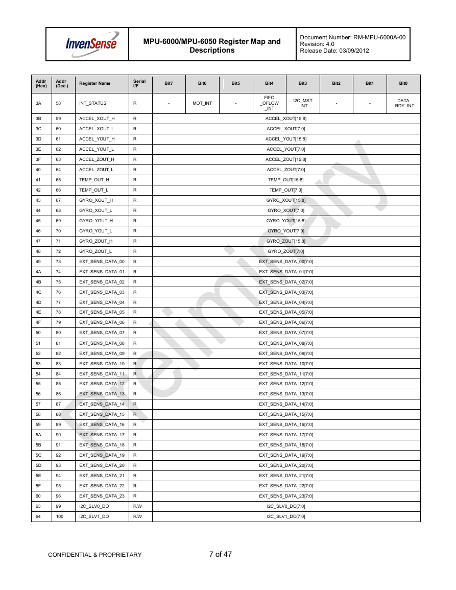
MPU-6000/MPU-6050 Register Map and Descriptions Document Number: RM-MPU-6000A-00 Revision: 4.0 Release Date: 03/09/2012 Addr (Hex) Addr (Dec.) Register Name Serial I/F Bit7 Bit6 Bit5 Bit4 Bit3 Bit2 Bit1 Bit0 - MOT_INT - 3A 3B 3C 3D 3E 3F 40 41 42 43 44 45 46 47 48 49 4A 4B 4C 4D 4E 4F 50 51 52 53 54 55 56 57 58 59 5A 5B 5C 5D 5E 5F 60 63 64 58 59 60 61 62 63 64 65 66 67 68 69 70 71 72 73 74 75 76 77 78 79 80 81 82 83 84 85 86 87 88 89 90 91 92 93 94 95 96 99 INT_STATUS ACCEL_XOUT_H ACCEL_XOUT_L ACCEL_YOUT_H ACCEL_YOUT_L ACCEL_ZOUT_H ACCEL_ZOUT_L TEMP_OUT_H TEMP_OUT_L GYRO_XOUT_H GYRO_XOUT_L GYRO_YOUT_H GYRO_YOUT_L GYRO_ZOUT_H GYRO_ZOUT_L EXT_SENS_DATA_00 EXT_SENS_DATA_01 EXT_SENS_DATA_02 EXT_SENS_DATA_03 EXT_SENS_DATA_04 EXT_SENS_DATA_05 EXT_SENS_DATA_06 EXT_SENS_DATA_07 EXT_SENS_DATA_08 EXT_SENS_DATA_09 EXT_SENS_DATA_10 EXT_SENS_DATA_11 EXT_SENS_DATA_12 EXT_SENS_DATA_13 EXT_SENS_DATA_14 EXT_SENS_DATA_15 EXT_SENS_DATA_16 EXT_SENS_DATA_17 EXT_SENS_DATA_18 EXT_SENS_DATA_19 EXT_SENS_DATA_20 EXT_SENS_DATA_21 EXT_SENS_DATA_22 EXT_SENS_DATA_23 I2C_SLV0_DO 100 I2C_SLV1_DO R R R R R R R R R R R R R R R R R R R R R R R R R R R R R R R R R R R R R R R R/W R/W FIFO _OFLOW _INT I2C_MST _INT - - DATA _RDY_INT ACCEL_XOUT[15:8] ACCEL_XOUT[7:0] ACCEL_YOUT[15:8] ACCEL_YOUT[7:0] ACCEL_ZOUT[15:8] ACCEL_ZOUT[7:0] TEMP_OUT[15:8] TEMP_OUT[7:0] GYRO_XOUT[15:8] GYRO_XOUT[7:0] GYRO_YOUT[15:8] GYRO_YOUT[7:0] GYRO_ZOUT[15:8] GYRO_ZOUT[7:0] EXT_SENS_DATA_00[7:0] EXT_SENS_DATA_01[7:0] EXT_SENS_DATA_02[7:0] EXT_SENS_DATA_03[7:0] EXT_SENS_DATA_04[7:0] EXT_SENS_DATA_05[7:0] EXT_SENS_DATA_06[7:0] EXT_SENS_DATA_07[7:0] EXT_SENS_DATA_08[7:0] EXT_SENS_DATA_09[7:0] EXT_SENS_DATA_10[7:0] EXT_SENS_DATA_11[7:0] EXT_SENS_DATA_12[7:0] EXT_SENS_DATA_13[7:0] EXT_SENS_DATA_14[7:0] EXT_SENS_DATA_15[7:0] EXT_SENS_DATA_16[7:0] EXT_SENS_DATA_17[7:0] EXT_SENS_DATA_18[7:0] EXT_SENS_DATA_19[7:0] EXT_SENS_DATA_20[7:0] EXT_SENS_DATA_21[7:0] EXT_SENS_DATA_22[7:0] EXT_SENS_DATA_23[7:0] I2C_SLV0_DO[7:0] I2C_SLV1_DO[7:0] CONFIDENTIAL & PROPRIETARY 7 of 47
MPU-6000/MPU-6050 Register Map and Descriptions Document Number: RM-MPU-6000A-00 Revision: 4.0 Release Date: 03/09/2012 Addr (Hex) Addr (Dec.) Register Name 65 66 67 68 69 6A 6B 6C 72 73 74 75 101 102 103 104 105 106 107 108 114 115 116 117 Serial I/F R/W R/W R/W R/W I2C_SLV2_DO I2C_SLV3_DO I2C_MST_DELAY_CT RL SIGNAL_PATH_RES ET MOT_DETECT_CTRL R/W USER_CTRL PWR_MGMT_1 PWR_MGMT_2 FIFO_COUNTH FIFO_COUNTL FIFO_R_W WHO_AM_I R/W R/W R/W R/W R/W R/W R Bit7 Bit6 Bit5 Bit4 Bit3 Bit2 Bit1 Bit0 I2C_SLV2_DO[7:0] I2C_SLV3_DO[7:0] I2C_SLV4 _DLY_EN I2C_SLV3 _DLY_EN - - - FIFO_EN - - - ACCEL_ON_DELAY[1:0] I2C_MST _EN I2C_IF _DIS I2C_SLV2 _DLY_EN GYRO _RESET I2C_SLV1 _DLY_EN ACCEL _RESET I2C_SLV0 _DLY_EN TEMP _RESET - - FIFO _RESET I2C_MST _RESET SIG_COND _RESET - - SLEEP CYCLE - TEMP_DIS CLKSEL[2:0] DELAY_ES _SHADOW - - - DEVICE _RESET LP_WAKE_CTRL[1:0] STBY_XA STBY_YA STBY_ZA STBY_XG STBY_YG STBY_ZG - FIFO_COUNT[15:8] FIFO_COUNT[7:0] FIFO_DATA[7:0] WHO_AM_I[6:1] - Register Names ending in _H and _L contain the high and low bytes, respectively, of an internal Note: register value. In the detailed register tables that follow, register names are in capital letters, while register values are in capital letters and italicized. For example, the ACCEL_XOUT_H register (Register 59) contains the 8 most significant bits, ACCEL_XOUT[15:8], of the 16-bit X-Axis accelerometer measurement, ACCEL_XOUT. The reset value is 0x00 for all registers other than the registers below. • Register 107: 0x40. • Register 117: 0x68. CONFIDENTIAL & PROPRIETARY 8 of 47
分享到:
收藏