OOTTTT22000011AA
220088--cchhaannnneell CCaappaacciittiivvee TToouucchh
SSeennssoorr DDrriivveerr ffoorr PPaassssiivvee MMaattrriixx
TToouucchh PPaanneell
PPrreelliimmiinnaarryy
OCT. 30, 2013
Version 0.1
ORISE Technology reserves the right to change this documentation without prior notice. Information provided by ORISE Technology is believed to be
accurate and reliable. However, ORISE Technology makes no warranty for any errors which may appear in this document. Contact ORISE Technology to
obtain the latest version of device specifications before placing your order. No responsibility is assumed by ORISE Technology for any infringement of patent
or other rights of third parties which may result from its use. In addition, ORISE Technology products are not authorized for use as critical components in life
support devices/ systems or aviation devices/systems, where a malfunction or failure of the product may reasonably be expected to result in significant injury to
the user, without the express written approval of ORISE Technology.
ORISE Tech Confidential For 新勵 Use Only�
Table of Contents
PPrreelliimmiinnaarryy
OTT2001A
PAGE
1. GENERAL DESCRIPTION .......................................................................................................................................................................... 3
2. FEATURES .................................................................................................................................................................................................. 3
3. BLOCK DIAGRAM ...................................................................................................................................................................................... 4
3.1. BLOCK FUNCTION .................................................................................................................................................................................. 4
3.1.1. System Interface ....................................................................................................................................................................... 5
3.1.2. Address Counter (AC) ............................................................................................................................................................... 5
3.1.3. TP buffer ................................................................................................................................................................................... 5
3.1.4. 8 bit SAR ADC .......................................................................................................................................................................... 5
3.1.5. Timing Controller ....................................................................................................................................................................... 5
3.1.6. Oscillator (OSC) ........................................................................................................................................................................ 5
3.1.7. Sensing Circuit .......................................................................................................................................................................... 5
3.1.8. Touch Power Supply Circuit ...................................................................................................................................................... 5
4. SIGNAL DESCRIPTIONS ............................................................................................................................................................................ 6
4.1. PIN DEFINITION ...................................................................................................................................................................................... 6
4.2. APPLICATION CIRCUIT ............................................................................................................................................................................ 7
4.2.1. Pump4X .................................................................................................................................................................................... 7
4.2.2. Pump2X .................................................................................................................................................................................... 7
4.3. BOM LIST ............................................................................................................................................................................................. 8
4.3.1. Pump4X .................................................................................................................................................................................... 8
4.3.2. Pump2X .................................................................................................................................................................................... 8
5. RESET FUNCTION ...................................................................................................................................................................................... 9
6. ELECTRICAL CHARACTERISTICS ......................................................................................................................................................... 10
6.1. ABSOLUTE MAXIMUM RATINGS: ............................................................................................................................................................ 10
6.2. DC CHARACTERISTICS ......................................................................................................................................................................... 10
6.3. AC CHARACTERISTICS ..........................................................................................................................................................................11
6.3.1. Clock Characteristics ...............................................................................................................................................................11
6.3.2. Clock-synchronized Serial Interface Timing Characteristics ....................................................................................................11
6.3.3. Reset Timing Characteristics (VDDIO=1.8~5.50V) ................................................................................................................. 12
7. POWER ON/OFF SEQUENCE .................................................................................................................................................................... 13
STANDBY IN / OUT SEQUENCE ....................................................................................................................................................................... 13
8. CHIP INFORMATION ( FOR COG) ............................................................................................................................................................. 14
8.1. PAD ASSIGNMENT ............................................................................................................................................................................... 14
8.2. PAD DIMENSIONS ................................................................................................................................................................................. 14
8.3. PAD LOCATIONS (FOR COG) ............................................................................................................................................................... 15
8.4. ALIGNMENT MARK ( FOR COG) ............................................................................................................................................................ 17
9. DISCLAIMER ............................................................................................................................................................................................. 18
10. REVISION HISTORY ................................................................................................................................................................................. 19
© ORISE Technology Co., Ltd.
Proprietary & Confidential
2
OCT. 30, 2013
Preliminary Version: 0.2
ORISE Tech Confidential For 新勵 Use Only�
208-CHANNEL CAPACITIVE
DRIVER FOR PASSIVE MATRIX
TOUCH PANEL
1. GENERAL DESCRIPTION
The OTT2001A, a 208 channels capacitive touch driver LSI, is
designed for up to 10.1” passive matrix touch panel. It includes
high speed 4 wire SPI interface to communicate with host
processor, 8 bit SAR-ADC to transfer charge variation to digital
code, and internal charge pump to supply 4X voltage of touch
sensing unit for passive matrix touch panel. Moreover, an
internal TP buffer, which can be used o store whole TP raw data,
is also built in OTT2001A. The TP buffer can reduce the latency
between host processor and OTT2001A.
PPrreelliimmiinnaarryy
OTT2001A
2. FEATURES
Supports passive matrix
to 10.1”
touch panel up
,
incorporating a 208-channel sensing drivers. Combined with
display gate driver, it can provide touch sensing signal to
touch electrode on PM panel.
8-bit SAR ADC converter to convert charge variation to
digital code when human’s finger touch the touch panel
Built-in 624 (208 x 3) bytes internal SRAM as TP buffer
System interfaces
4 wire( CSX, DI, DO, CLK), high-speed interfaces, max to
15Mhz to support high speed data transfer between host
processor and touch driver
Power supply
I/O interface supply voltage (VDDIO): 1.8 ~ 5.5 V, typical
3.3V.
Analog power supply voltage (VCI): 2.8 ~ 5.5 V, typical
3.3V
On-chip power management system
Power saving mode to reduce power consumption when
no touched (STBY function)
Built-in Charge Pump circuits
Sensing driver voltage level: VDDA-GND=8V ~ 12V.
Built-in internal oscillator and hardware reset
External Component
4 Capacitors for Power and Charge Pump circuits.
© ORISE Technology Co., Ltd.
Proprietary & Confidential
3
OCT. 30, 2013
Preliminary Version: 0.2
ORISE Tech Confidential For 新勵 Use Only�
Preliminary
OTT2001A
SPI
Interface
TP Frame
Buffer
Power & clock
Power
Control
OSC
Pump
Timing
Control
8
AFE
8 bit ADC
TCON
Scan IF
PM Detector
Command
Set
Signal
processing
PANEL
3. BLOCK DIAGRAM
3.1. Block Function
CSB
SCL
SDI
SDO
HS, VS
Power
Cap
Cap
© ORISE Technology Co., Ltd.
Proprietary & Confidential
4
OCT. 30, 2013
Preliminary Version: 0.2
ORISE Tech Confidential For 新勵 Use Only�
Preliminary
OTT2001A
System Interface
3.1.1.
The OTT2001A supports SPI system high-speed interfaces:
- 4-pin 8-bits Serial Peripheral Interface (SPI)
The OTT2001A has three data registers, 1) index register (IR), 2) write-data register (WDR) and 3) read-data register (RDR). The IR
register is used to store index information from control registers. The WDR register is used to temporarily store data to be written for
register control and internal TP buffer. The RDR register is used to temporarily store data read from the TP buffer. When touch data is
written to the internal TP buffer from MCU engine, the data is first written to the WDR and then automatically written to the internal TP
buffer by internal operation. When touch data read operation is executed, touch data is read via the RDR from the internal TP buffer.
Therefore, invalid data is first read out to the data bus when the OTT2001A executes the 1st read operation. Thus, valid data can be read
out after the OTT2001A executes the 2nd read operation.
Table 3-1 Register Selection (Serial Peripheral Interface)
Start byte (SPI)
R/W
0
1
0
1
RS
0
0
1
1
Function
Write an index to IR
Reserved
Write into control registers and the internal TP buffer via WDR
Read from the internal TP buffer and registers via RDR
TP buffer
8 bit SAR ADC
Address Counter (AC)
3.1.2.
OTT2001A includes an address counter (AC) gives an address to
the TP buffer. The address in the AC is automatically updated plus
1.
3.1.3.
OTT2001A includes a TP buffer which has the capacity of 624
(208 x 3 ) bytes.
3.1.4.
OTT2001A has a 8-bit resolution SAR A/D converter, which can
transfer capacitance variance to max 256 touch scale for touch
application.
3.1.5.
OTT2001A has a timing controller which can generates a timing
signal for internal circuits operation such as sensing timing, RAM
accessing timing, etc.
Timing Controller
Sensing Circuit
Oscillator (OSC)
3.1.6.
The OTT2001A include an internal oscillator, which generates RC
oscillation without an external resistor. The frequency can be
adjusted through the register setting. In standby mode, RC
oscillation is halted to reduce power consumption.
3.1.7.
OTT2001A consists of 208-output sensing circuit (C1 ~ C208).
When human’s fingers touch the touch panel, touch Data would be
accumulated or integrated by the sensing circuit. After sensing or
amplifying operation, the analog signal would be transferred to
digital code by SAR ADC. Then all TP data would be stored into
TP buffer.
3.1.8.
The touch power supply circuit generates the voltage levels VDRV.
All this voltages can be adjusted by register setting.
Touch Power Supply Circuit
© ORISE Technology Co., Ltd.
Proprietary & Confidential
5
OCT. 30, 2013
Preliminary Version: 0.2
ORISE Tech Confidential For 新勵 Use Only�
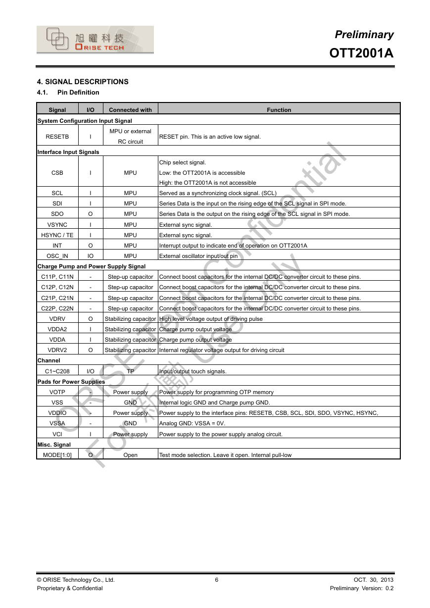
4. SIGNAL DESCRIPTIONS
4.1. Pin Definition
Signal
I/O
Connected with
System Configuration Input Signal
RESETB
I
Interface Input Signals
MPU or external
RC circuit
Function
RESET pin. This is an active low signal.
Preliminary
OTT2001A
CSB
SCL
SDI
SDO
VSYNC
HSYNC / TE
INT
OSC_IN
I
I
I
O
I
I
O
IO
MPU
MPU
MPU
MPU
MPU
MPU
MPU
MPU
Chip select signal.
Low: the OTT2001A is accessible
High: the OTT2001A is not accessible
Served as a synchronizing clock signal. (SCL)
Series Data is the input on the rising edge of the SCL signal in SPI mode.
Series Data is the output on the rising edge of the SCL signal in SPI mode.
External sync signal.
External sync signal.
Interrupt output to indicate end of operation on OTT2001A
External oscillator input/out pin
Charge Pump and Power Supply Signal
C11P, C11N
C12P, C12N
C21P, C21N
C22P, C22N
VDRV
VDDA2
VDDA
VDRV2
Channel
-
-
-
-
O
I
I
O
Step-up capacitor Connect boost capacitors for the internal DC/DC converter circuit to these pins.
Step-up capacitor Connect boost capacitors for the internal DC/DC converter circuit to these pins.
Step-up capacitor Connect boost capacitors for the internal DC/DC converter circuit to these pins.
Step-up capacitor Connect boost capacitors for the internal DC/DC converter circuit to these pins.
Stabilizing capacitor High level voltage output of driving pulse
Stabilizing capacitor Charge pump output voltage
Stabilizing capacitor Charge pump output voltage
Stabilizing capacitor Internal regulator voltage output for driving circuit
C1~C208
I/O
TP
Input/output touch signals.
Power supply
GND
Power supply
GND
Power supply
Power supply for programming OTP memory
Internal logic GND and Charge pump GND.
Power supply to the interface pins: RESETB, CSB, SCL, SDI, SDO, VSYNC, HSYNC,
Analog GND: VSSA = 0V.
Power supply to the power supply analog circuit.
Open
Test mode selection. Leave it open. Internal pull-low
Pads for Power Supplies
VOTP
VSS
VDDIO
VSSA
VCI
Misc. Signal
MODE[1:0]
-
-
-
-
I
O
© ORISE Technology Co., Ltd.
Proprietary & Confidential
6
OCT. 30, 2013
Preliminary Version: 0.2
ORISE Tech Confidential For 新勵 Use Only�
Preliminary
OTT2001A
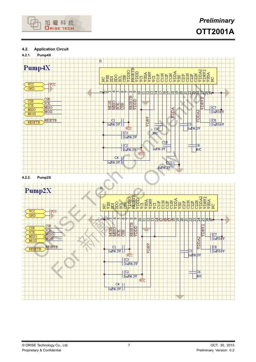
4.2. Application Circuit
4.2.1.
Pump4X
4.2.2.
Pump2X
© ORISE Technology Co., Ltd.
Proprietary & Confidential
7
OCT. 30, 2013
Preliminary Version: 0.2
ORISE Tech Confidential For 新勵 Use Only�
Preliminary
OTT2001A
OTT2001A BOM LISTS
Max. Ability
6.3V
6.3V
6.3V
6.3V
6.3V
6.3V
16V
16V
6.3V
6.3V
6.3V
OTT2001A BOM LISTS
Max. Ability
6.3V
6.3V
6.3V
6.3V
6.3V
6.3V
16V
16V
Value
1.0uF
1.0uF
1.0uF
1.0uF
1.0uF
1.0uF
1.0uF
1.0uF
1.0uF
1.0uF
1.0uF
Value
1.0uF
1.0uF
1.0uF
1.0uF
1.0uF
1.0uF
1.0uF
1.0uF
Note
I/O Power
Analog Power
Digital Power
VDDA Pump
VDDA2 Pump
VDDA2 Pump (Option)
VDDA2 Pump
VDDA2 Pump
VDDA Pump (Option)
VDDA Pump
VDDA Pump
Note
I/O Power
Analog Power
Digital Power
VDDA Pump
VDDA2 Pump
VDDA2 Pump (Option)
VDDA2 Pump
VDDA2 Pump
4.3. BOM List
4.3.1.
Pump4X
NO.
1
2
3
4
5
6
7
8
9
10
11
Signal Name
VDDIO
VCI
VDDD
VDRV
C21P/C21N
C22P/C22N
VDRV2
VDDA2
C11P/C11N
C12P/C12N
VDDA
4.3.2.
Pump2X
Signal Name
VDDIO
VCI
VDDD
VDRV
C21P/C21N
C22P/C22N
VDRV2
VDDA2
NO.
1
2
3
4
5
6
7
8
© ORISE Technology Co., Ltd.
Proprietary & Confidential
8
OCT. 30, 2013
Preliminary Version: 0.2
ORISE Tech Confidential For 新勵 Use Only�
