logo资料库

AN2784(4STM32 FSMC学习资料).pdf

第1页 / 共30页
第2页 / 共30页
第3页 / 共30页
第4页 / 共30页
第5页 / 共30页
第6页 / 共30页
第7页 / 共30页
第8页 / 共30页
资料共30页,剩余部分请下载后查看
1 Overview of the STM32F10xxx flexible static memory controller
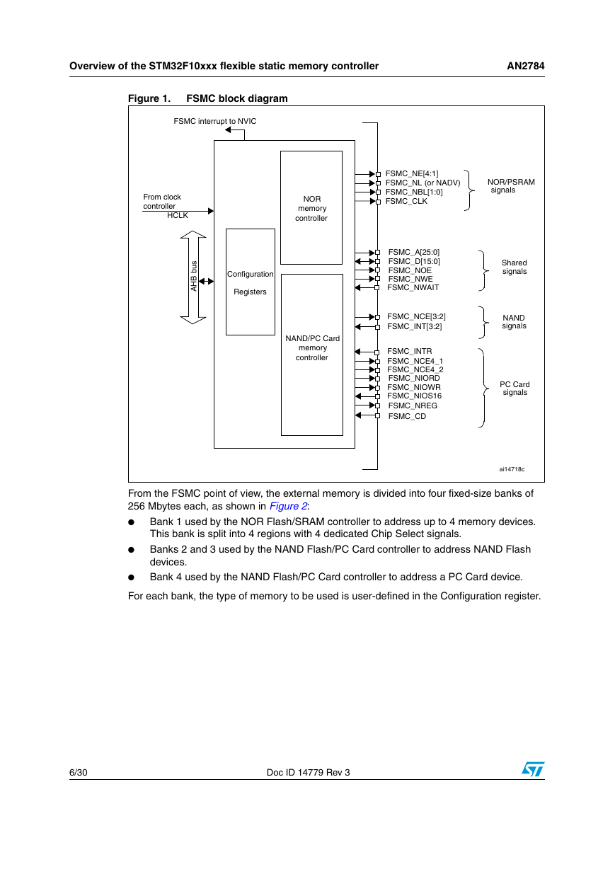
Figure 1. FSMC block diagram
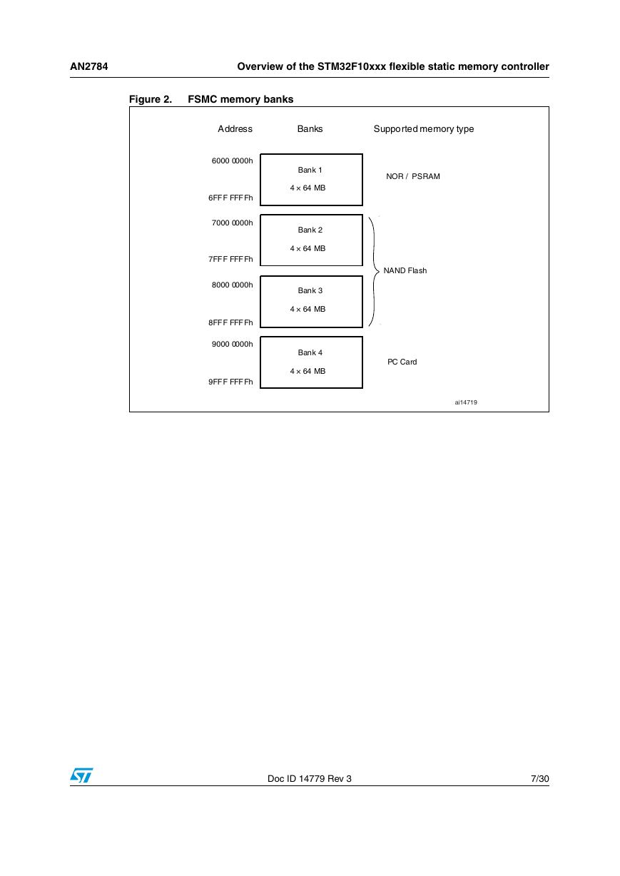
Figure 2. FSMC memory banks
2 Interfacing with a nonmultiplexed, asynchronous 16-bit NOR Flash memory
2.1 FSMC configuration
Figure 3. Asynchronous NOR Flash read access timing
Figure 4. Asynchronous NOR Flash write access timing
2.1.1 Typical use of the FSMC to interface with a NOR Flash memory
2.2 Timing computation
Table 1. NOR Flash memory timings
Table 2. STM32F10xxx parameters
2.3 Hardware connection
Table 3. M29W128FL signal to FSMC pin correspondence
Figure 5. 16-bit NOR Flash: M29W128FL/GL connection to STM32F10xxx
2.4 Code execution from an external NOR Flash memory
3 Interfacing with a nonmultiplexed, asynchronous 16- bit SRAM
3.1 FSMC configuration
Figure 6. SRAM asynchronous read access timing
Figure 7. SRAM asynchronous write access timing
3.1.1 Typical use of the FSMC to interface with an SRAM
3.2 Timing computation
Table 4. SRAM timings
3.3 Hardware connection
Table 5. IS61WV51216BLL signal to FSMC pin correspondence
Figure 8. 16-bit SRAM: IS61WV51216BLL connection to STM32F10xxx
3.4 Using the external SRAM as a data memory
4 Interfacing with an 8-bit NAND Flash memory
Figure 9. FSMC NAND bank sections
4.1 FSMC configuration
Figure 10. NAND memory access timing
4.1.1 Typical use of the FSMC to interface with a NAND memory
4.2 Timing computation
Table 6. NAND Flash memory timings
4.3 Hardware connection
Table 7. NAND512W3A signal to FSMC pin correspondence
Figure 11. 8-bit NAND Flash: NAND512W3A2C/NAND512W3A2B connection to STM32F10xxx
4.4 Error correction code computation
4.4.1 Error correction code (ECC) computation overview
4.4.2 Error detection
Figure 12. Error detection flowchart
5 STM32F10xxx FSMC configuration in 100-pin packages
5.1 Interfacing the FSMC with a NAND Flash memory
Table 8. NAND Flash memory connection to the FSMC
5.2 Interfacing the FSMC with a NOR Flash memory
Table 9. NOR Flash memory connection to the FSMC
6 Revision history
Table 10. Document revision history
AN2784 Application note Using the high-density STM32F10xxx FSMC peripheral to drive external memories Introduction This application note describes how to use the High-density STM32F10xxx FSMC (flexible static memory controller) peripheral to drive a set of external memories. To that aim, it gives an overview of the STM32F10xxx FSMC controller. Then it provides memory interfacing examples that include the typical FSMC configuration, the timing computation method and the hardware connection. This application note is based on memories mounted on the STM3210E-EVAL, which is the evaluation board for High-density STM32F10xxx devices. The used memories are a 16-bit asynchronous NOR Flash memory, an 8-bit NAND Flash memory and a 16-bit asynchronous SRAM. The STM32F10xxx firmware library, the different memory drivers and examples of use for each of the memory types used in this application note, are available for download from the STMicroelectronics website: www.st.com/mcu. April 2009 Doc ID 14779 Rev 3 1/30 www.st.com
Contents Contents AN2784 1 2 3 4 5 Overview of the STM32F10xxx flexible static memory controller . . . . 5 Interfacing with a nonmultiplexed, asynchronous 16-bit NOR Flash memory . . . . . . . . . . . . . . . . . . . . . . . . . . . . . . . . . . . . 8 FSMC configuration . . . . . . . . . . . . . . . . . . . . . . . . . . . . . . . . . . . . . . . . . . 8 2.1 2.1.1 Typical use of the FSMC to interface with a NOR Flash memory . . . . . 10 Timing computation . . . . . . . . . . . . . . . . . . . . . . . . . . . . . . . . . . . . . . . . . 10 Hardware connection . . . . . . . . . . . . . . . . . . . . . . . . . . . . . . . . . . . . . . . . 12 Code execution from an external NOR Flash memory . . . . . . . . . . . . . . . 14 2.2 2.3 2.4 Interfacing with a nonmultiplexed, asynchronous 16-bit SRAM . . . . . 15 FSMC configuration . . . . . . . . . . . . . . . . . . . . . . . . . . . . . . . . . . . . . . . . . 15 3.1 3.1.1 Typical use of the FSMC to interface with an SRAM . . . . . . . . . . . . . . . 16 Timing computation . . . . . . . . . . . . . . . . . . . . . . . . . . . . . . . . . . . . . . . . . 16 Hardware connection . . . . . . . . . . . . . . . . . . . . . . . . . . . . . . . . . . . . . . . . 17 Using the external SRAM as a data memory . . . . . . . . . . . . . . . . . . . . . . 18 3.2 3.3 3.4 Interfacing with an 8-bit NAND Flash memory . . . . . . . . . . . . . . . . . . . 19 FSMC configuration . . . . . . . . . . . . . . . . . . . . . . . . . . . . . . . . . . . . . . . . . 20 4.1 4.1.1 Typical use of the FSMC to interface with a NAND memory . . . . . . . . . 21 Timing computation . . . . . . . . . . . . . . . . . . . . . . . . . . . . . . . . . . . . . . . . . 22 Hardware connection . . . . . . . . . . . . . . . . . . . . . . . . . . . . . . . . . . . . . . . . 24 Error correction code computation . . . . . . . . . . . . . . . . . . . . . . . . . . . . . . 25 Error correction code (ECC) computation overview . . . . . . . . . . . . . . . . 25 4.4.1 4.4.2 Error detection . . . . . . . . . . . . . . . . . . . . . . . . . . . . . . . . . . . . . . . . . . . . 26 4.2 4.3 4.4 STM32F10xxx FSMC configuration in 100-pin packages . . . . . . . . . . 27 Interfacing the FSMC with a NAND Flash memory . . . . . . . . . . . . . . . . . 27 5.1 5.2 Interfacing the FSMC with a NOR Flash memory . . . . . . . . . . . . . . . . . . 28 6 Revision history . . . . . . . . . . . . . . . . . . . . . . . . . . . . . . . . . . . . . . . . . . . 29 2/30 Doc ID 14779 Rev 3
AN2784 List of tables List of tables Table 1. Table 2. Table 3. Table 4. Table 5. Table 6. Table 7. Table 8. Table 9. Table 10. NOR Flash memory timings . . . . . . . . . . . . . . . . . . . . . . . . . . . . . . . . . . . . . . . . . . . . . . . . 11 STM32F10xxx parameters . . . . . . . . . . . . . . . . . . . . . . . . . . . . . . . . . . . . . . . . . . . . . . . . . 11 M29W128FL signal to FSMC pin correspondence . . . . . . . . . . . . . . . . . . . . . . . . . . . . . . . 12 SRAM timings . . . . . . . . . . . . . . . . . . . . . . . . . . . . . . . . . . . . . . . . . . . . . . . . . . . . . . . . . . . 17 IS61WV51216BLL signal to FSMC pin correspondence . . . . . . . . . . . . . . . . . . . . . . . . . . 17 NAND Flash memory timings . . . . . . . . . . . . . . . . . . . . . . . . . . . . . . . . . . . . . . . . . . . . . . . 23 NAND512W3A signal to FSMC pin correspondence . . . . . . . . . . . . . . . . . . . . . . . . . . . . . 24 NAND Flash memory connection to the FSMC . . . . . . . . . . . . . . . . . . . . . . . . . . . . . . . . . 27 NOR Flash memory connection to the FSMC. . . . . . . . . . . . . . . . . . . . . . . . . . . . . . . . . . . 28 Document revision history . . . . . . . . . . . . . . . . . . . . . . . . . . . . . . . . . . . . . . . . . . . . . . . . . 29 Doc ID 14779 Rev 3 3/30
List of figures List of figures AN2784 FSMC block diagram . . . . . . . . . . . . . . . . . . . . . . . . . . . . . . . . . . . . . . . . . . . . . . . . . . . . . . 6 Figure 1. FSMC memory banks . . . . . . . . . . . . . . . . . . . . . . . . . . . . . . . . . . . . . . . . . . . . . . . . . . . . . . 7 Figure 2. Asynchronous NOR Flash read access timing . . . . . . . . . . . . . . . . . . . . . . . . . . . . . . . . . . . 9 Figure 3. Asynchronous NOR Flash write access timing . . . . . . . . . . . . . . . . . . . . . . . . . . . . . . . . . . . 9 Figure 4. 16-bit NOR Flash: M29W128FL/GL connection to STM32F10xxx . . . . . . . . . . . . . . . . . . . 13 Figure 5. SRAM asynchronous read access timing . . . . . . . . . . . . . . . . . . . . . . . . . . . . . . . . . . . . . . 15 Figure 6. SRAM asynchronous write access timing. . . . . . . . . . . . . . . . . . . . . . . . . . . . . . . . . . . . . . 16 Figure 7. 16-bit SRAM: IS61WV51216BLL connection to STM32F10xxx . . . . . . . . . . . . . . . . . . . . . 18 Figure 8. Figure 9. FSMC NAND bank sections . . . . . . . . . . . . . . . . . . . . . . . . . . . . . . . . . . . . . . . . . . . . . . . . 19 Figure 10. NAND memory access timing . . . . . . . . . . . . . . . . . . . . . . . . . . . . . . . . . . . . . . . . . . . . . . . 21 Figure 11. 8-bit NAND Flash: NAND512W3A2C/NAND512W3A2B connection to STM32F10xxx. . . . . . . . . . . . . . . . . . . . . . . . . . . . . . . . . . . . . . . . . . . . . . . . . . . . . . . . . . . 25 Figure 12. Error detection flowchart. . . . . . . . . . . . . . . . . . . . . . . . . . . . . . . . . . . . . . . . . . . . . . . . . . . 26 4/30 Doc ID 14779 Rev 3
AN2784 1 Overview of the STM32F10xxx flexible static memory controller Overview of the STM32F10xxx flexible static memory controller The flexible static memory controller (FSMC) is an external memory controller embedded in High-density STM32F10xxx devices. Using it, the STM32F10xxx microcontroller can interface with a variety of memories, including SRAM, NOR Flash and NAND Flash memories. The FSMC contains two types of controller: ● a NOR Flash/SRAM controller to interface with NOR Flash memories, SRAMs and PSRAMs a NAND Flash/PC Card controller to interface with NAND Flash, PC Card, CF and CF+ memories ● ● ● ● The controllers generate the appropriate signal timings to drive all these memories: ● 16 data lines to interface with 8-bit or 16-bit memory width 26 address lines to interface with up to 64 Mbytes memory size 5 independent memory Chip Select pins A set of control signals adapted for every type of memory: – – to control read/ write operations to actively communicate with memories which provide the Ready/Busy signals and the interrupt signals to interface with the PC Card in all possible configurations: PC card memory, PC card I/O, true IDE – Figure 1 illustrates the FSMC block diagram. Doc ID 14779 Rev 3 5/30
Overview of the STM32F10xxx flexible static memory controller AN2784 Figure 1. FSMC block diagram FSMC interrupt to NVIC From clock controller HCLK NOR memory controller FSMC_NE[4:1] FSMC_NL (or NADV) FSMC_NBL[1:0] FSMC_CLK NOR/PSRAM signals s u b B H A Configuration Registers NAND/PC Card memory controller FSMC_A[25:0] FSMC_D[15:0] FSMC_NOE FSMC_NWE FSMC_NWAIT FSMC_NCE[3:2] FSMC_INT[3:2] FSMC_INTR FSMC_NCE4_1 FSMC_NCE4_2 FSMC_NIORD FSMC_NIOWR FSMC_NIOS16 FSMC_NREG FSMC_CD Shared signals NAND signals PC Card signals ai14718c From the FSMC point of view, the external memory is divided into four fixed-size banks of 256 Mbytes each, as shown in Figure 2: ● Bank 1 used by the NOR Flash/SRAM controller to address up to 4 memory devices. This bank is split into 4 regions with 4 dedicated Chip Select signals. Banks 2 and 3 used by the NAND Flash/PC Card controller to address NAND Flash devices. Bank 4 used by the NAND Flash/PC Card controller to address a PC Card device. ● ● For each bank, the type of memory to be used is user-defined in the Configuration register. 6/30 Doc ID 14779 Rev 3
AN2784 Overview of the STM32F10xxx flexible static memory controller Figure 2. FSMC memory banks Address Banks Supported memory type 6000 0000h 6FFF FFFFh 7000 0000h 7FFF FFFFh 8000 0000h 8FFF FFFFh 9000 0000h 9FFF FFFFh Bank 1 4 × 64 MB Bank 2 4 × 64 MB Bank 3 4 × 64 MB Bank 4 4 × 64 MB NOR / PSRAM NAND Flash PC Card ai14719 Doc ID 14779 Rev 3 7/30
Interfacing with a nonmultiplexed, asynchronous 16-bit NOR Flash memory AN2784 2 2.1 Interfacing with a nonmultiplexed, asynchronous 16-bit NOR Flash memory FSMC configuration To control a NOR Flash memory, the FSMC provides the following possible features: ● Select the bank to be used to map the NOR Flash memory: there are 4 independent banks which can be used to interface with NOR Flash/SRAM/PSRAM memories, each bank has a separate Chip Select pin. Enable or disable the address/data multiplexing feature Select the memory type to be used: NOR Flash/SRAM/PSRAM Define the external memory databus width: 8/16 bits Enable or disable the burst access mode for synchronous NOR Flash memories Configure the use of the wait signal: enable/disable, polarity setting and timing configuration. Enable or disable the extended mode: this mode is used to access the memory with a different timing configuration for read and write operations. ● ● ● ● ● ● As the NOR Flash/PSRAM controller can support asynchronous and synchronous memories, the user should select only the used parameters depending on the memory characteristics. The FSMC also provides the possibility of programming several parameters to correctly interface with the external memory. Depending on the memory type, some parameters are not used. ● ● ● In the case where an external asynchronous memory is used, the user has to compute and set the following parameters depending on the information in the memory datasheet: ● ADDSET: address setup time ADDHOLD: address hold time DATAST: data setup time ACCMOD: access mode This parameter gives the FSMC the flexibility to access a wide variety of asynchronous static memories. There are four extended access modes that allow write access while reading the memory with different timings, if the memory supports this kind of feature. When the extended mode is enabled, the FSMC_BTR register is used for read operations and the FSMC_BWR register is used for write operations. In the case where a synchronous memory is used, the user has to compute and set the following parameters: ● CLKDIV: clock divide ratio DATLAT: data latency ● Note that NOR Flash memory read operations can be synchronous if the memory supports this mode, while write operations usually remain asynchronous. When programming a synchronous NOR Flash memory, the memory automatically switches between the synchronous and the asynchronous mode, so in this case, all parameters have to be set correctly. 8/30 Doc ID 14779 Rev 3
分享到:
收藏