logo资料库

SIM900A_Hardware Design_V1.03.pdf

第1页 / 共48页
第2页 / 共48页
第3页 / 共48页
第4页 / 共48页
第5页 / 共48页
第6页 / 共48页
第7页 / 共48页
第8页 / 共48页
资料共48页,剩余部分请下载后查看
Contents
Version History
1 Introduction
2 SIM900A Overview
2.1 SIM900A Key Features
2.2 Operating Modes
2.3 SIM900A Functional Diagram
3 Package Information
3.1 Pin out Diagram
3.2 Pin Description
3.3 Package Dimensions
4 Application Interface
4.1 Power Supply
4.1.1 Minimizing Voltage Drop of VBAT
4.1.2 Monitoring Power Supply
4.2 Power on/down Scenarios
4.2.1 Power on SIM900A
4.2.2 Power down SIM900A
4.2.2.1 Power down SIM900A by the PWRKEY Pin
4.2.2.2 Power down SIM900A by AT Command
4.2.2.3 Over-voltage or Under-voltage Power down
4.2.2.4 Over-temperature or Under-temperature Power down
4.2.3 Restart SIM900A by PWRKEY Pin
4.3 Power Saving Mode
4.3.2 Sleep Mode 1 (AT+CSCLK=1)
4.3.3 Wake Up SIM900A from Sleep Mode 1 (AT+CSCLK=1)
4.3.4 Sleep Mode 2 (AT+CSCLK=2)
4.3.5 Wake Up SIM900A from Sleep Mode 2 (AT+CSCLK=2)
4.4 RTC Backup
4.5 Serial Interfaces
4.5.1 Function of Serial Port and Debug Port
4.5.2 Software Upgrade and Debug
4.6 Audio Interfaces
4.6.1 Speaker Interface Configuration
4.6.2 Microphone Interfaces Configuration
4.6.3 Earphone Interface Configuration
4.6.4 Audio Electronic Characteristics
4.7 SIM Card Interface
4.7.1 SIM Card Application
4.7.2 Design Considerations for SIM Card Holder
4.8 LCD Display/SPI Interface
4.9 Keypad Interface
4.10 ADC
4.11 RI Behaviours
4.12 Network Status Indication
4.13 General Purpose Input/Output (GPIO)
4.14 External Reset
4.15 PWM
4.16 I2C Bus
4.17 Antenna Interface
5 Electrical, Reliability and Radio Characteristics
5.1 Absolute Maximum Ratings
5.2 Recommended Operating Conditions
5.3 Digital Interface Characteristics
5.4 SIM Card Interface Characteristics
5.5 VDD_EXT Characteristics
5.6 SIM_VDD Characteristics
5.7 VRTC Characteristics
5.8 Current Consumption (VBAT = 3.8V)
5.9 Electro-Static Discharge
5.10 Radio Characteristics
5.10.1 Module RF Output Power
5.10.2 Module RF Receive Sensitivity
5.10.3 Module Operating Frequencies
6 Manufacturing
6.1 Top and Bottom View of SIM900A
6.2 Typical Solder Reflow Profile
Appendix
A. Related Documents
B. Terms and Abbreviations
C. Safety Caution
SIM900A_Hardware Design_V1.03
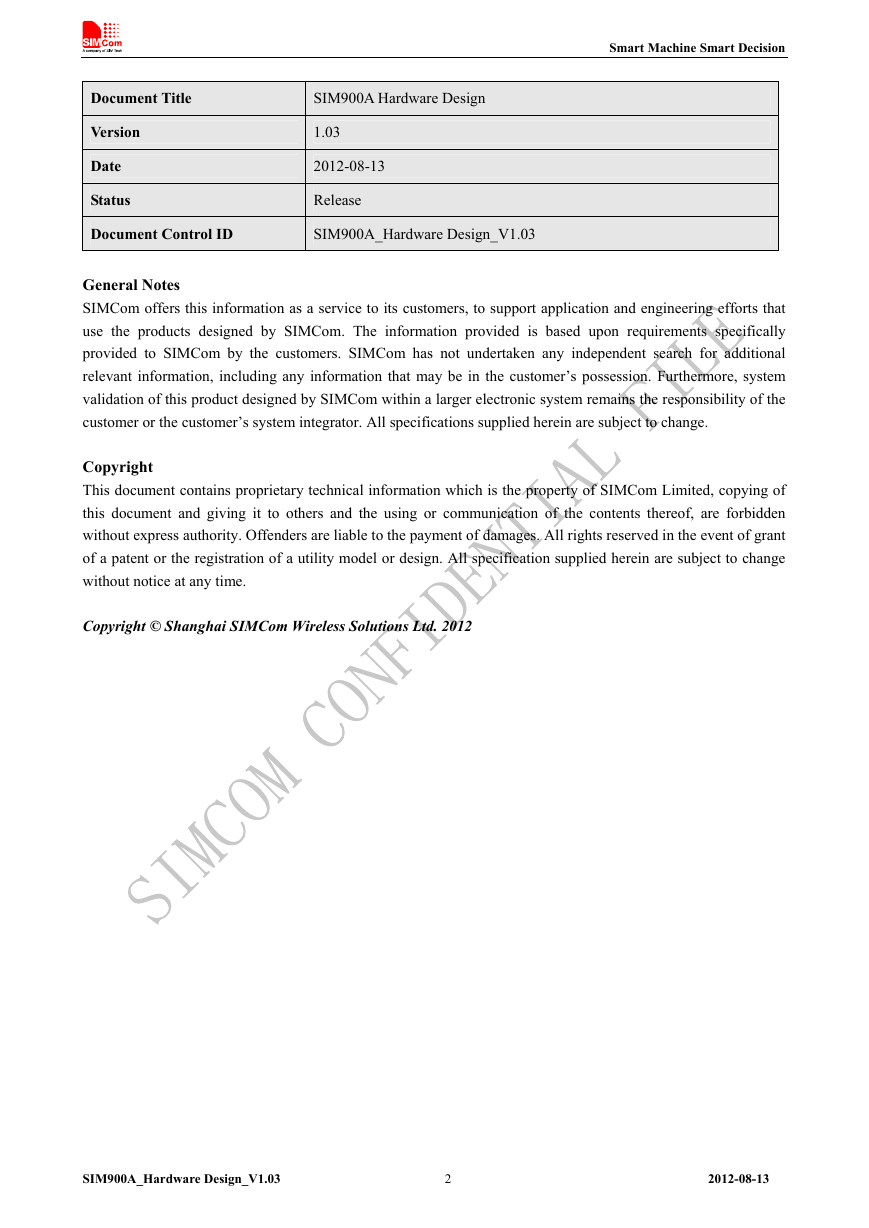
Smart Machine Smart Decision Document Title SIM900A Hardware Design Version Date Status 1.03 2012-08-13 Release Document Control ID SIM900A_Hardware Design_V1.03 General Notes SIMCom offers this information as a service to its customers, to support application and engineering efforts that use the products designed by SIMCom. The information provided is based upon requirements specifically provided to SIMCom by the customers. SIMCom has not undertaken any independent search for additional relevant information, including any information that may be in the customer’s possession. Furthermore, system validation of this product designed by SIMCom within a larger electronic system remains the responsibility of the customer or the customer’s system integrator. All specifications supplied herein are subject to change. Copyright This document contains proprietary technical information which is the property of SIMCom Limited, copying of this document and giving it to others and the using or communication of the contents thereof, are forbidden without express authority. Offenders are liable to the payment of damages. All rights reserved in the event of grant of a patent or the registration of a utility model or design. All specification supplied herein are subject to change without notice at any time. Copyright © Shanghai SIMCom Wireless Solutions Ltd. 2012 SIM900A_Hardware Design_V1.03 2 2012-08-13
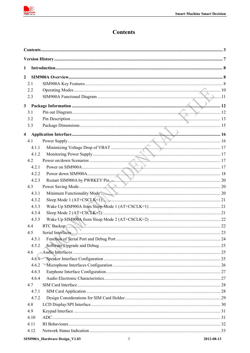
Smart Machine Smart Decision Contents Contents.................................................................................................................................................................... 3 Version History........................................................................................................................................................ 7 1 Introduction....................................................................................................................................................... 8 2 SIM900A Overview........................................................................................................................................... 8 SIM900A Key Features............................................................................................................................ 8 Operating Modes .................................................................................................................................... 10 SIM900A Functional Diagram ................................................................................................................11 2.1 2.2 2.3 3 Package Information ...................................................................................................................................... 12 Pin out Diagram...................................................................................................................................... 12 Pin Description ....................................................................................................................................... 13 Package Dimensions............................................................................................................................... 15 3.1 3.2 3.3 4.1 4.2 4.3 4 Application Interface...................................................................................................................................... 16 Power Supply.......................................................................................................................................... 16 4.1.1 Minimizing Voltage Drop of VBAT................................................................................................... 17 4.1.2 Monitoring Power Supply................................................................................................................... 17 Power on/down Scenarios ...................................................................................................................... 17 Power on SIM900A............................................................................................................................. 17 4.2.1 4.2.2 Power down SIM900A........................................................................................................................ 18 4.2.3 Restart SIM900A by PWRKEY Pin.................................................................................................... 20 Power Saving Mode................................................................................................................................ 20 4.3.1 Minimum Functionality Mode ............................................................................................................ 20 4.3.2 Sleep Mode 1 (AT+CSCLK=1) .......................................................................................................... 21 4.3.3 Wake Up SIM900A from Sleep Mode 1 (AT+CSCLK=1) ................................................................ 21 4.3.4 Sleep Mode 2 (AT+CSCLK=2) .......................................................................................................... 21 4.3.5 Wake Up SIM900A from Sleep Mode 2 (AT+CSCLK=2) ................................................................ 22 RTC Backup ........................................................................................................................................... 22 Serial Interfaces...................................................................................................................................... 23 Function of Serial Port and Debug Port .............................................................................................. 24 Software Upgrade and Debug ............................................................................................................. 25 Audio Interfaces ..................................................................................................................................... 25 4.6.1 Speaker Interface Configuration ......................................................................................................... 25 4.6.2 Microphone Interfaces Configuration ................................................................................................. 26 4.6.3 Earphone Interface Configuration....................................................................................................... 27 4.6.4 Audio Electronic Characteristics......................................................................................................... 27 SIM Card Interface ................................................................................................................................. 28 4.7.1 SIM Card Application......................................................................................................................... 28 4.7.2 Design Considerations for SIM Card Holder...................................................................................... 29 LCD Display/SPI Interface..................................................................................................................... 30 4.8 4.9 Keypad Interface .................................................................................................................................... 31 4.10 ADC........................................................................................................................................................ 31 4.11 RI Behaviours......................................................................................................................................... 32 4.12 Network Status Indication ...................................................................................................................... 33 4.5.1 4.5.2 4.7 4.4 4.5 4.6 SIM900A_Hardware Design_V1.03 3 2012-08-13
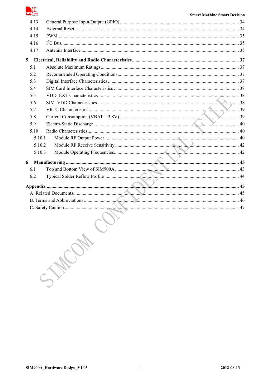
Smart Machine Smart Decision 4.13 General Purpose Input/Output (GPIO) ................................................................................................... 34 External Reset......................................................................................................................................... 34 4.14 4.15 PWM ...................................................................................................................................................... 35 I2C Bus.................................................................................................................................................... 35 4.16 4.17 Antenna Interface ................................................................................................................................... 35 5.1 5.2 5.3 5.4 5.5 5.6 5.7 5.8 5.9 5.10 5 Electrical, Reliability and Radio Characteristics......................................................................................... 37 Absolute Maximum Ratings................................................................................................................... 37 Recommended Operating Conditions..................................................................................................... 37 Digital Interface Characteristics ............................................................................................................. 37 SIM Card Interface Characteristics ........................................................................................................ 38 VDD_EXT Characteristics ..................................................................................................................... 38 SIM_VDD Characteristics...................................................................................................................... 38 VRTC Characteristics............................................................................................................................. 39 Current Consumption (VBAT = 3.8V) ................................................................................................... 39 Electro-Static Discharge ......................................................................................................................... 40 Radio Characteristics.............................................................................................................................. 40 5.10.1 Module RF Output Power................................................................................................................ 40 5.10.2 Module RF Receive Sensitivity ....................................................................................................... 42 5.10.3 Module Operating Frequencies........................................................................................................ 42 6 Manufacturing ................................................................................................................................................ 43 Top and Bottom View of SIM900A ....................................................................................................... 43 Typical Solder Reflow Profile................................................................................................................ 44 6.1 6.2 Appendix ................................................................................................................................................................ 45 A. Related Documents.......................................................................................................................................... 45 B. Terms and Abbreviations ................................................................................................................................. 46 C. Safety Caution ................................................................................................................................................. 47 SIM900A_Hardware Design_V1.03 4 2012-08-13
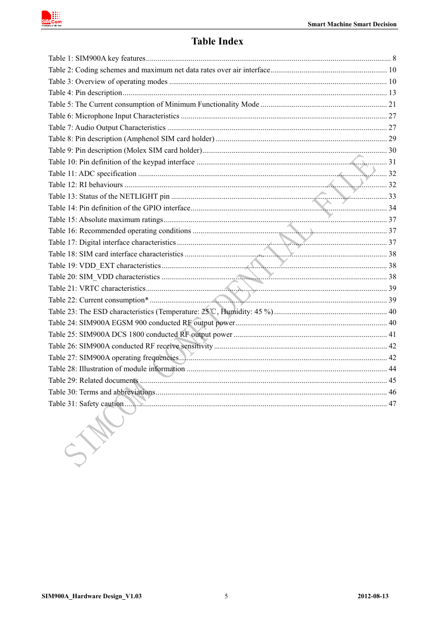
Smart Machine Smart Decision Table Index Table 1: SIM900A key features.............................................................................................................................. 8 Table 2: Coding schemes and maximum net data rates over air interface............................................................ 10 Table 3: Overview of operating modes ................................................................................................................ 10 Table 4: Pin description........................................................................................................................................ 13 Table 5: The Current consumption of Minimum Functionality Mode ................................................................. 21 Table 6: Microphone Input Characteristics .......................................................................................................... 27 Table 7: Audio Output Characteristics ................................................................................................................. 27 Table 8: Pin description (Amphenol SIM card holder) ........................................................................................ 29 Table 9: Pin description (Molex SIM card holder)............................................................................................... 30 Table 10: Pin definition of the keypad interface .................................................................................................. 31 Table 11: ADC specification ................................................................................................................................ 32 Table 12: RI behaviours ....................................................................................................................................... 32 Table 13: Status of the NETLIGHT pin ............................................................................................................... 33 Table 14: Pin definition of the GPIO interface..................................................................................................... 34 Table 15: Absolute maximum ratings................................................................................................................... 37 Table 16: Recommended operating conditions .................................................................................................... 37 Table 17: Digital interface characteristics ............................................................................................................ 37 Table 18: SIM card interface characteristics ........................................................................................................ 38 Table 19: VDD_EXT characteristics.................................................................................................................... 38 Table 20: SIM_VDD characteristics .................................................................................................................... 38 Table 21: VRTC characteristics............................................................................................................................ 39 Table 22: Current consumption* .......................................................................................................................... 39 Table 23: The ESD characteristics (Temperature: 25℃, Humidity: 45 %) .......................................................... 40 Table 24: SIM900A EGSM 900 conducted RF output power.............................................................................. 40 Table 25: SIM900A DCS 1800 conducted RF output power ............................................................................... 41 Table 26: SIM900A conducted RF receive sensitivity ......................................................................................... 42 Table 27: SIM900A operating frequencies........................................................................................................... 42 Table 28: Illustration of module information ....................................................................................................... 44 Table 29: Related documents ............................................................................................................................... 45 Table 30: Terms and abbreviations....................................................................................................................... 46 Table 31: Safety caution....................................................................................................................................... 47 SIM900A_Hardware Design_V1.03 5 2012-08-13
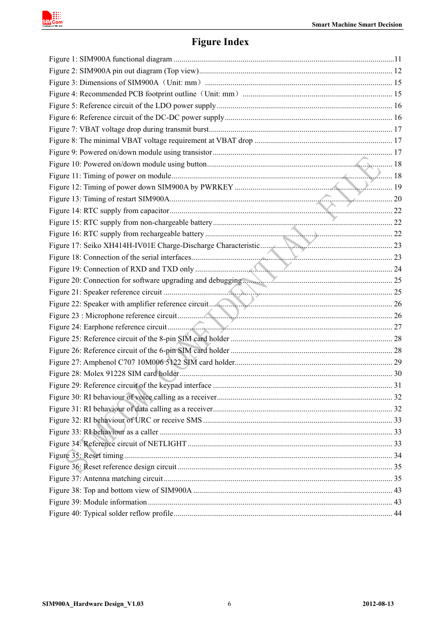
Smart Machine Smart Decision Figure Index Figure 1: SIM900A functional diagram ................................................................................................................11 Figure 2: SIM900A pin out diagram (Top view).................................................................................................. 12 Figure 3: Dimensions of SIM900A(Unit: mm)............................................................................................... 15 Figure 4: Recommended PCB footprint outline(Unit: mm)............................................................................ 15 Figure 5: Reference circuit of the LDO power supply......................................................................................... 16 Figure 6: Reference circuit of the DC-DC power supply..................................................................................... 16 Figure 7: VBAT voltage drop during transmit burst............................................................................................. 17 Figure 8: The minimal VBAT voltage requirement at VBAT drop ...................................................................... 17 Figure 9: Powered on/down module using transistor........................................................................................... 17 Figure 10: Powered on/down module using button.............................................................................................. 18 Figure 11: Timing of power on module................................................................................................................ 18 Figure 12: Timing of power down SIM900A by PWRKEY ................................................................................ 19 Figure 13: Timing of restart SIM900A................................................................................................................. 20 Figure 14: RTC supply from capacitor................................................................................................................. 22 Figure 15: RTC supply from non-chargeable battery........................................................................................... 22 Figure 16: RTC supply from rechargeable battery ............................................................................................... 22 Figure 17: Seiko XH414H-IV01E Charge-Discharge Characteristic................................................................... 23 Figure 18: Connection of the serial interfaces...................................................................................................... 23 Figure 19: Connection of RXD and TXD only .................................................................................................... 24 Figure 20: Connection for software upgrading and debugging............................................................................ 25 Figure 21: Speaker reference circuit .................................................................................................................... 25 Figure 22: Speaker with amplifier reference circuit............................................................................................. 26 Figure 23 : Microphone reference circuit............................................................................................................. 26 Figure 24: Earphone reference circuit.................................................................................................................. 27 Figure 25: Reference circuit of the 8-pin SIM card holder .................................................................................. 28 Figure 26: Reference circuit of the 6-pin SIM card holder .................................................................................. 28 Figure 27: Amphenol C707 10M006 5122 SIM card holder................................................................................ 29 Figure 28: Molex 91228 SIM card holder............................................................................................................ 30 Figure 29: Reference circuit of the keypad interface ........................................................................................... 31 Figure 30: RI behaviour of voice calling as a receiver......................................................................................... 32 Figure 31: RI behaviour of data calling as a receiver........................................................................................... 32 Figure 32: RI behaviour of URC or receive SMS ................................................................................................ 33 Figure 33: RI behaviour as a caller ...................................................................................................................... 33 Figure 34: Reference circuit of NETLIGHT........................................................................................................ 33 Figure 35: Reset timing........................................................................................................................................ 34 Figure 36: Reset reference design circuit............................................................................................................. 35 Figure 37: Antenna matching circuit.................................................................................................................... 35 Figure 38: Top and bottom view of SIM900A ..................................................................................................... 43 Figure 39: Module information............................................................................................................................ 43 Figure 40: Typical solder reflow profile............................................................................................................... 44 SIM900A_Hardware Design_V1.03 6 2012-08-13
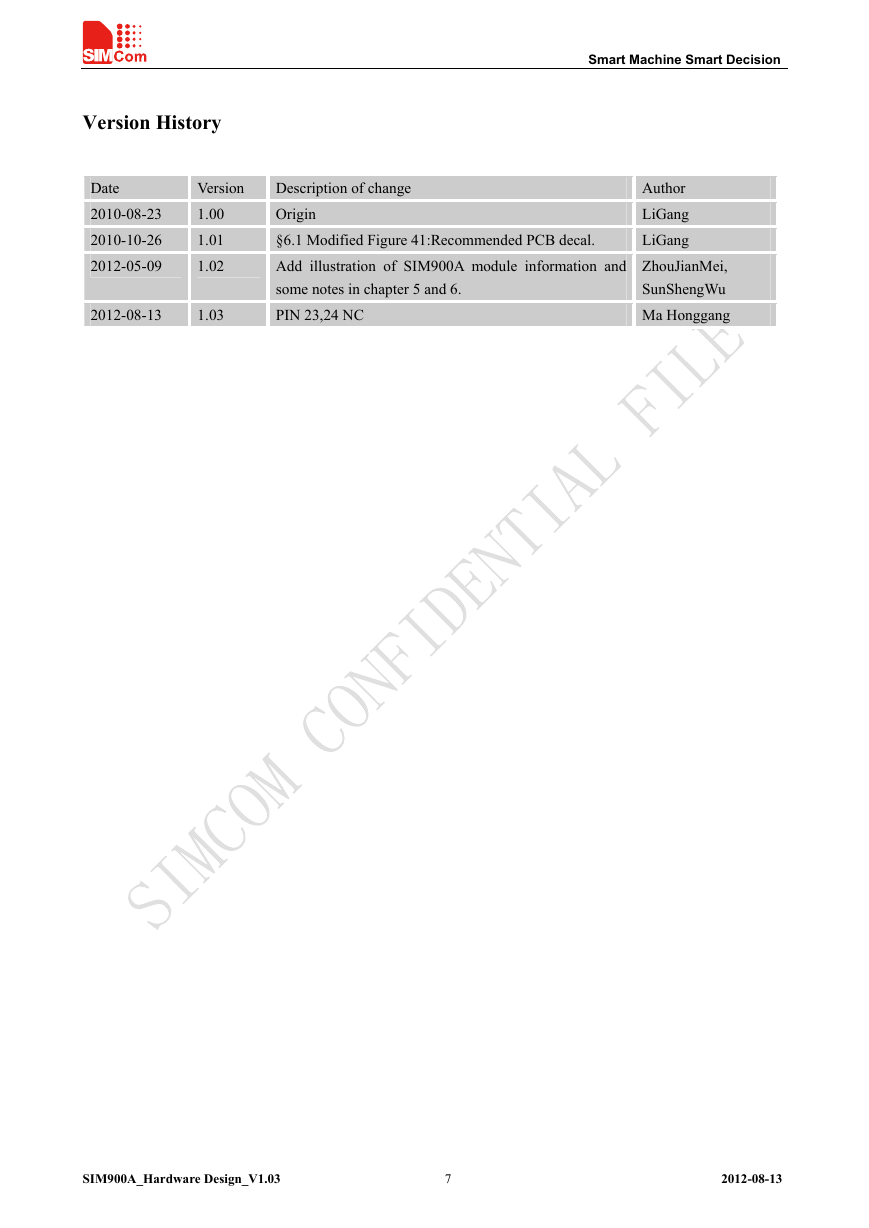
Smart Machine Smart Decision Version History Date 2010-08-23 2010-10-26 2012-05-09 Version 1.00 1.01 1.02 2012-08-13 1.03 Description of change Origin §6.1 Modified Figure 41:Recommended PCB decal. Add illustration of SIM900A module information and some notes in chapter 5 and 6. PIN 23,24 NC Author LiGang LiGang ZhouJianMei, SunShengWu Ma Honggang SIM900A_Hardware Design_V1.03 7 2012-08-13
Smart Machine Smart Decision 1 Introduction This document describes SIM900A hardware interface in great detail. This document can help user to quickly understand SIM900A interface specifications, electrical and mechanical details. With the help of this document and other SIM900A application notes, user guide, users can use SIM900A to design various applications quickly. 2 SIM900A Overview Designed for global market, SIM900A is a dual-band GSM/GPRS module that works on frequencies EGSM 900MHz and DCS 1800MHz. SIM900A features GPRS multi-slot class 10/ class 8 (optional) and supports the GPRS coding schemes CS-1, CS-2, CS-3 and CS-4. With a tiny configuration of 24*24*3mm, SIM900A can meet almost all the space requirements in user applications, such as M2M, smart phone, PDA and other mobile devices. SIM900A has 68 SMT pads, and provides all hardware interfaces between the module and customers’ boards. Serial port and debug port can help user easily develop user’s applications. Audio channel which includes a microphone input and a receiver output. Programmable general purpose input and output. The keypad and SPI display interfaces will give users the flexibility to develop customized applications. SIM900A is designed with power saving technique so that the current consumption is as low as 1.0mA in sleep mode. SIM900A integrates TCP/IP protocol and extended TCP/IP AT commands which are very useful for data transfer applications. For details about TCP/IP applications, please refer to document [2]. 2.1 SIM900A Key Features Table 1: SIM900A key features Feature Power supply Power saving Frequency bands Transmitting power GPRS connectivity Implementation 3.2V ~ 4.8V Typical power consumption in sleep mode is 1.0mA ( BS-PA-MFRMS=9 ) SIM900A Dual-band: EGSM 900, DCS 1800. SIM900A can search the 2 frequency bands automatically. The frequency bands also can be set by AT command “AT+CBAND”. For details, please refer to document [1]. Compliant to GSM Phase 2/2+ Class 4 (2W) at EGSM 900 Class 1 (1W) at DCS 1800 GPRS multi-slot class 10(default) GPRS multi-slot class 8 (option) SIM900A_Hardware Design_V1.03 8 2012-08-13
分享到:
收藏