logo资料库

CC2430芯片数据手册.pdf

第1页 / 共225页
第2页 / 共225页
第3页 / 共225页
第4页 / 共225页
第5页 / 共225页
第6页 / 共225页
第7页 / 共225页
第8页 / 共225页
资料共225页,剩余部分请下载后查看
Abbreviations
References
Register conventions
Features (continued from front page)
High-Performance and Low-Power 8051-Compatible Microcontroll
Up to 128 KB Non-volatile Program Memory and 2 x 4 KB Data M
Hardware AES Encryption/Decryption
Peripheral Features
Low Power
802.15.4 MAC hardware support
Integrated 2.4GHz DSSS Digital Radio
Absolute Maximum Ratings
Operating Conditions
Electrical Specifications
General Characteristics
RF Receive Section
RF Transmit Section
32 MHz Crystal Oscillator
32.768 kHz Crystal Oscillator
Low Power RC Oscillator
High Speed RC Oscillator
Frequency Synthesizer Characteristics
Analog Temperature Sensor
8-14 bit ADC
Control AC Characteristics
SPI AC Characteristics
Debug Interface AC Characteristics
Port Outputs AC Characteristics
Timer Inputs AC Characteristics
DC Characteristics
Pin and I/O Port Configuration
Circuit Description
CPU and Peripherals
Radio
Power Management
Application Circuit
Input / output matching
Bias resistors
Crystal
Voltage regulators
Power supply decoupling and filtering
8051 CPU
8051 CPU Introduction
Reset
Memory
Memory Map
Memory Space
Data Pointers
XDATA Memory Access
SFR Registers
CPU Registers
Registers R0-R7
Program Status Word
Accumulator
B Register
Stack Pointer
Instruction Set Summary
Interrupts
Interrupt Masking
Interrupt Processing
Interrupt Priority
Oscillators and clocks
Debug Interface
Debug Mode
Debug Communication
Debug Commands
Debug Lock Bit
Debug Configuration
Debug Status
Hardware Breakpoints
Flash Programming
RAM
Flash Memory
Memory Arbiter
Peripherals
I/O ports
General Purpose I/O
General Purpose I/O Interrupts
General Purpose I/O DMA
Peripheral I/O
USART0
USART1
Timer 1
Timer 3
Timer 4
ADC
Debug interface
32.768 kHz XOSC input
Unused I/O pins
I/O registers
DMA Controller
DMA Operation
DMA Configuration Parameters
Source Address
Destination Address
Transfer Count
VLEN Setting
Trigger Event
Source and Destination Increment
DMA Transfer Mode
DMA Priority
Byte or Word transfers
Interrupt mask
Mode 8 setting
DMA Configuration Setup
Stopping DMA Transfers
DMA Interrupts
DMA Configuration Data Structure
DMA registers
16-bit Timer, Timer1
16-bit Timer Counter
Timer 1 Operation
Free-running Mode
Modulo Mode
Up/down Mode
Channel Mode Control
Input Capture Mode
RF Event Capture
Output Compare Mode
Timer 1 Interrupts
DMA Triggers
Timer 1 Registers
MAC Timer (Timer 2)
Timer Operation
General
Up Counter
Timer overflow
Timer delta increment
Timer Compare
Capture Input
Overflow count
Overflow count compare
Interrupts
DMA Triggers
Timer start/stop synchronization
General
Timer synchronous stop
Timer synchronous start
Timer 2 Registers
Sleep Timer
Timer Operation
General
Timer Compare
8-bit Timer 3 and Timer 4
8-bit Timer Counter
Timer 3/4 Mode Control
Channel Mode Control
Input Capture Mode
Output Compare Mode
Timer 3 and 4 interrupts
Timer 3 and Timer 4 DMA triggers
Timer 3 and 4 registers
ADC
ADC Introduction
ADC Operation
ADC Core
ADC conversion sequences
ADC Inputs
ADC Operating Modes
ADC Conversion Results
ADC Reference Voltage
ADC Conversion Timing
ADC Interrupts
ADC DMA Triggers
ADC Registers
Random Generator
Introduction
Random Generator Operation
Semi random sequence generation
Seeding
CRC16
Registers
AES Coprocessor
AES Operation
Key and IV
Padding of input data
Interface to CPU
Modes of operation
CBC-MAC
CCM mode
Sharing the AES coprocessor between layers
AES Interrupts
AES DMA Triggers
AES Registers
Power Management
Power Management Introduction
PM0
PM1
PM2
PM3
Power Management Control
System clock
High-speed oscillators
32.768 kHz oscillators
Timer Tick generation
Data Retention
Power Management Registers
Power On Reset and Brown Out Detector
Watchdog Timer
Watchdog mode
Timer mode
Watchdog Timer Example
Watchdog Timer Register
USART
UART mode
UART Transmit
UART Receive
UART Hardware Flow Control
UART Character Format
SPI Mode
SPI Master Operation
SPI Slave Operation
Baud Rate Generation
USART flushing
USART Interrupts
USART DMA Triggers
USART Registers
FLASH Controller
Flash Write
DMA Flash Write
CPU Flash Write
Flash Page Erase
Flash Lock Protection
Flash Write Timing
Flash DMA trigger
Flash Controller Registers
Radio
IEEE 802.15.4 Modulation Format
Command strobes
RF Registers
Interrupts
Interrupt registers
FIFO access
DMA
Receive mode
RXFIFO overflow
Transmit mode
General control and status
Demodulator, Symbol Synchronizer and Data Decision
Frame Format
Synchronization header
Length field
MAC protocol data unit
Frame check sequence
RF Data Buffering
Buffered transmit mode
Buffered receive mode
Address Recognition
Acknowledge Frames
Radio control state machine
MAC Security Operations (Encryption and Authentication)
Linear IF and AGC Settings
RSSI / Energy Detection
Link Quality Indication
Clear Channel Assessment
Frequency and Channel Programming
VCO and PLL Self-Calibration
VCO
PLL self-calibration
Output Power Programming
Input / Output Matching
Transmitter Test Modes
Unmodulated carrier
Modulated spectrum
System Considerations and Guidelines
SRD regulations
Frequency hopping and multi-channel systems
Data burst transmissions
Crystal accuracy and drift
Communication robustness
Communication security
Low cost systems
Battery operated systems
BER / PER measurements
PCB Layout Recommendation
Antenna Considerations
CSMA/CA Strobe Processor
Instruction Memory
Data Registers
Program Execution
Interrupt Requests
Random Number Instruction
Running CSP Programs
Instruction Set Summary
Instruction Set Definition
DECZ
DECY
INCY
INCMAXY
RANDXY
INT
WAITX
WAIT W
WEVENT
LABEL
RPT C
SKIP S, C
STOP
SNOP
STXCALN
SRXON
STXON
STXONCCA
SRFOFF
SFLUSHRX
SFLUSHTX
SACK
SACKPEND
ISSTOP
ISSTART
ISTXCALN
ISRXON
ISTXON
ISTXONCCA
ISRFOFF
ISFLUSHRX
ISFLUSHTX
ISACK
ISACKPEND
Example programs
Radio Registers
Radio Test Output Signals
Voltage Regulators
Voltage Regulators Power-on
Evaluation Software
Register overview
Package Description (QLP 48)
Recommended PCB layout for package (QLP 48)
Package thermal properties
Soldering information
Plastic tube specification
Carrier tape and reel specification
Ordering Information
General Information
Document History
Product Status Definitions
Disclaimer
Trademarks
Life Support Policy
Address Information
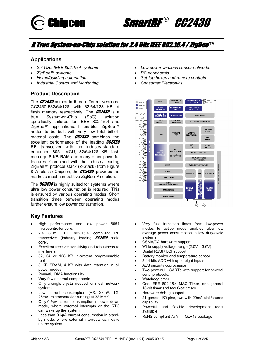
Chipcon SmartRF ® CC2430 A True System-on-Chip solution for 2.4 GHz IEEE 802.15.4 / ZigBee™ Applications • 2.4 GHz IEEE 802.15.4 systems • ZigBee™ systems • Home/building automation • Industrial Control and Monitoring • Low power wireless sensor networks • PC peripherals • Set-top boxes and remote controls • Consumer Electronics (SoC) System-on-Chip Product Description The CC2430 comes in three different versions: CC2430-F32/64/128, with 32/64/128 KB of flash memory respectively. The CC2430 is a true solution specifically tailored for IEEE 802.15.4 and ZigBee™ applications. It enables ZigBee™ nodes to be built with very low total bill-of- material costs. The CC2430 combines the excellent performance of the leading CC2420 RF industry-standard enhanced 8051 MCU, 32/64/128 KB flash memory, 8 KB RAM and many other powerful features. Combined with the industry leading ZigBee™ protocol stack (Z-Stack) from Figure 8 Wireless / Chipcon, the CC2430 provides the market’s most competitive ZigBee™ solution. The CC2430 is highly suited for systems where ultra low power consumption is required. This is ensured by various operating modes. Short transition times between operating modes further ensure low power consumption. transceiver with an Key Features • High performance and microcontroller core. 2.4 GHz transceiver core). • • • low power 8051 IEEE 802.15.4 compliant RF (industry radio leading CC2420 • Excellent receiver sensitivity and robustness to interferers 32, 64 or 128 KB in-system programmable flash 8 KB SRAM, 4 KB with data retention in all power modes • • Powerful DMA functionality • Very few external components • Only a single crystal needed for mesh network systems Low current consumption (RX: 27mA, TX: 25mA, microcontroller running at 32 MHz) • Only 0.9µA current consumption in power-down mode, where external interrupts or the RTC can wake up the system Less than 0.6µA current consumption in stand- by mode, where external interrupts can wake up the system • • Very fast transition low-power modes low average power consumption in low duty-cycle systems to active mode enables ultra times from • CSMA/CA hardware support. • Wide supply voltage range (2.0V – 3.6V) • Digital RSSI / LQI support • Battery monitor and temperature sensor. • • AES security coprocessor • 8-14 bits ADC with up to eight inputs Two powerful USARTs with support for several serial protocols. • Watchdog timer • One IEEE 802.15.4 MAC Timer, one general 16-bit timer and two 8-bit timers • Hardware debug support • 21 general I/O pins, two with 20mA sink/source capability • Powerful and flexible development tools available • RoHS compliant 7x7mm QLP48 package Chipcon AS SmartRF® CC2430 PRELIMINARY (rev. 1.01) 2005-09-15 Page 1 of 225
Chipcon SmartRF ® CC2430 Table Of Contents ABBREVIATIONS.....................................................................................................................5 1 REFERENCES ...........................................................................................................................7 2 REGISTER CONVENTIONS...................................................................................................8 3 FEATURES (CONTINUED FROM FRONT PAGE).............................................................9 4 HIGH-PERFORMANCE AND LOW-POWER 8051-COMPATIBLE MICROCONTROLLER .......................9 4.1 UP TO 128 KB NON-VOLATILE PROGRAM MEMORY AND 2 X 4 KB DATA MEMORY.....................9 4.2 HARDWARE AES ENCRYPTION/DECRYPTION................................................................................9 4.3 PERIPHERAL FEATURES.................................................................................................................9 4.4 LOW POWER..................................................................................................................................9 4.5 802.15.4 MAC HARDWARE SUPPORT ............................................................................................9 4.6 INTEGRATED 2.4GHZ DSSS DIGITAL RADIO ................................................................................9 4.7 ABSOLUTE MAXIMUM RATINGS.....................................................................................10 5 OPERATING CONDITIONS .................................................................................................10 6 ELECTRICAL SPECIFICATIONS.......................................................................................11 7 GENERAL CHARACTERISTICS ......................................................................................................12 7.1 RF RECEIVE SECTION..................................................................................................................13 7.2 RF TRANSMIT SECTION...............................................................................................................14 7.3 32 MHZ CRYSTAL OSCILLATOR..................................................................................................14 7.4 32.768 KHZ CRYSTAL OSCILLATOR ............................................................................................15 7.5 LOW POWER RC OSCILLATOR.....................................................................................................15 7.6 HIGH SPEED RC OSCILLATOR .....................................................................................................16 7.7 FREQUENCY SYNTHESIZER CHARACTERISTICS............................................................................16 7.8 ANALOG TEMPERATURE SENSOR ................................................................................................17 7.9 7.10 8-14 BIT ADC..............................................................................................................................17 7.11 CONTROL AC CHARACTERISTICS................................................................................................18 7.12 SPI AC CHARACTERISTICS..........................................................................................................19 7.13 DEBUG INTERFACE AC CHARACTERISTICS .................................................................................20 7.14 PORT OUTPUTS AC CHARACTERISTICS .......................................................................................20 7.15 TIMER INPUTS AC CHARACTERISTICS.........................................................................................21 7.16 DC CHARACTERISTICS ................................................................................................................21 8 PIN AND I/O PORT CONFIGURATION .............................................................................22 CIRCUIT DESCRIPTION ......................................................................................................24 9 CPU AND PERIPHERALS ..............................................................................................................25 9.1 9.2 RADIO .........................................................................................................................................26 POWER MANAGEMENT......................................................................................................27 10 APPLICATION CIRCUIT......................................................................................................28 11 11.1 INPUT / OUTPUT MATCHING .........................................................................................................28 11.2 BIAS RESISTORS...........................................................................................................................28 11.3 CRYSTAL.....................................................................................................................................28 11.4 VOLTAGE REGULATORS...............................................................................................................28 11.5 POWER SUPPLY DECOUPLING AND FILTERING..............................................................................28 12 8051 CPU...................................................................................................................................31 12.1 8051 CPU INTRODUCTION ..........................................................................................................31 12.2 RESET..........................................................................................................................................31 12.3 MEMORY.....................................................................................................................................31 12.4 SFR REGISTERS...........................................................................................................................42 12.5 CPU REGISTERS..........................................................................................................................45 12.6 INSTRUCTION SET SUMMARY......................................................................................................47 12.7 INTERRUPTS ................................................................................................................................51 Chipcon AS SmartRF® CC2430 PRELIMINARY (rev. 1.01) 2005-09-15 Page 2 of 225
Chipcon SmartRF ® CC2430 12.8 OSCILLATORS AND CLOCKS.........................................................................................................61 12.9 DEBUG INTERFACE......................................................................................................................61 12.10 RAM...................................................................................................................................65 FLASH MEMORY..................................................................................................................65 12.11 MEMORY ARBITER ..............................................................................................................65 12.12 13 PERIPHERALS........................................................................................................................68 13.1 I/O PORTS....................................................................................................................................68 13.2 DMA CONTROLLER ....................................................................................................................85 13.3 16-BIT TIMER, TIMER1 ................................................................................................................96 13.4 MAC TIMER (TIMER 2) .............................................................................................................108 13.5 SLEEP TIMER.............................................................................................................................115 13.6 8-BIT TIMER 3 AND TIMER 4......................................................................................................116 13.7 ADC..........................................................................................................................................125 13.8 RANDOM GENERATOR...............................................................................................................131 13.9 AES COPROCESSOR...................................................................................................................133 13.10 POWER MANAGEMENT ......................................................................................................138 POWER ON RESET AND BROWN OUT DETECTOR...............................................................141 13.11 WATCHDOG TIMER............................................................................................................142 13.12 13.13 USART.............................................................................................................................144 13.14 FLASH CONTROLLER .......................................................................................................154 RADIO.....................................................................................................................................161 14 14.1 IEEE 802.15.4 MODULATION FORMAT .....................................................................................162 14.2 COMMAND STROBES..................................................................................................................163 14.3 RF REGISTERS...........................................................................................................................163 14.4 INTERRUPTS ..............................................................................................................................163 14.5 FIFO ACCESS.............................................................................................................................166 14.6 DMA.........................................................................................................................................167 14.7 RECEIVE MODE..........................................................................................................................167 14.8 RXFIFO OVERFLOW .................................................................................................................168 14.9 TRANSMIT MODE .......................................................................................................................169 14.10 GENERAL CONTROL AND STATUS ......................................................................................169 14.11 DEMODULATOR, SYMBOL SYNCHRONIZER AND DATA DECISION......................................170 FRAME FORMAT ................................................................................................................170 14.12 SYNCHRONIZATION HEADER..............................................................................................171 14.13 14.14 LENGTH FIELD ...................................................................................................................172 14.15 MAC PROTOCOL DATA UNIT .............................................................................................172 14.16 FRAME CHECK SEQUENCE..................................................................................................172 RF DATA BUFFERING ........................................................................................................173 14.17 14.18 ADDRESS RECOGNITION....................................................................................................174 14.19 ACKNOWLEDGE FRAMES...................................................................................................175 14.20 RADIO CONTROL STATE MACHINE .....................................................................................176 MAC SECURITY OPERATIONS (ENCRYPTION AND AUTHENTICATION)..............................179 14.21 LINEAR IF AND AGC SETTINGS ........................................................................................179 14.22 14.23 RSSI / ENERGY DETECTION ..............................................................................................179 14.24 LINK QUALITY INDICATION...............................................................................................179 CLEAR CHANNEL ASSESSMENT.........................................................................................180 14.25 FREQUENCY AND CHANNEL PROGRAMMING.....................................................................180 14.26 14.27 VCO AND PLL SELF-CALIBRATION ..................................................................................181 14.28 OUTPUT POWER PROGRAMMING .......................................................................................181 14.29 INPUT / OUTPUT MATCHING ..............................................................................................181 TRANSMITTER TEST MODES..............................................................................................182 14.30 14.31 SYSTEM CONSIDERATIONS AND GUIDELINES ....................................................................184 14.32 PCB LAYOUT RECOMMENDATION ....................................................................................186 14.33 ANTENNA CONSIDERATIONS .............................................................................................186 CSMA/CA STROBE PROCESSOR .......................................................................................187 14.34 14.35 RADIO REGISTERS .............................................................................................................199 Chipcon AS SmartRF® CC2430 PRELIMINARY (rev. 1.01) 2005-09-15 Page 3 of 225
Chipcon SmartRF ® CC2430 RADIO TEST OUTPUT SIGNALS......................................................................................216 15 VOLTAGE REGULATORS .................................................................................................217 16 16.1 VOLTAGE REGULATORS POWER-ON..........................................................................................217 EVALUATION SOFTWARE ...............................................................................................217 17 18 REGISTER OVERVIEW......................................................................................................218 19 PACKAGE DESCRIPTION (QLP 48).................................................................................221 19.1 RECOMMENDED PCB LAYOUT FOR PACKAGE (QLP 48)............................................................222 19.2 PACKAGE THERMAL PROPERTIES...............................................................................................222 19.3 SOLDERING INFORMATION.........................................................................................................222 19.4 PLASTIC TUBE SPECIFICATION ...................................................................................................222 19.5 CARRIER TAPE AND REEL SPECIFICATION ..................................................................................223 20 ORDERING INFORMATION..............................................................................................223 21 GENERAL INFORMATION................................................................................................223 21.1 DOCUMENT HISTORY ................................................................................................................223 21.2 PRODUCT STATUS DEFINITIONS ................................................................................................224 21.3 DISCLAIMER..............................................................................................................................224 21.4 TRADEMARKS............................................................................................................................224 21.5 LIFE SUPPORT POLICY...............................................................................................................224 22 ADDRESS INFORMATION.................................................................................................225 Chipcon AS SmartRF® CC2430 PRELIMINARY (rev. 1.01) 2005-09-15 Page 4 of 225
Chipcon SmartRF ® CC2430 1 Abbreviations ADC AES AGC ARIB SmartRF® CC2430 PRELIMINARY (rev. 1.01) 2005-09-15 Page 5 of 225 Analog to Digital Converter Advanced Encryption Standard Automatic Gain Control Association of Radio Industries and Businesses Binary Coded Decimal Bit Error Rate Brown Out Detector Bill of Materials Cipher Block Chaining Cipher Block Chaining Message Authentication Code Clear Channel Assessment Counter mode + CBC-MAC Cipher Feedback Code of Federal Regulations Complementary Metal Oxide Semiconductor Central Processing Unit Cyclic Redundancy Check Carrier Sense Multiple Access with Collision Avoidance CSMA/CA Strobe Processor Counter mode (encryption) Continuous Wave Digital to Analog Converter Direct Current Direct Memory Access Delta Sigma Modulator Direct Sequence Spread Spectrum Electronic Code Book (encryption) Evaluation Module Electro Static Discharge Equivalent Series Resistance European Telecommunications Standards Institute Error Vector Magnitude Federal Communications Commission Frame Control Field Frame Check Sequence FIFO and Frame Control First In First Out High Speed Serial Data BCD BER BOD BOM CBC CBC-MAC CCA CCM CFB CFR CMOS CPU CRC CSMA-CA CSP CTR CW DAC DC DMA DSM DSSS ECB EM ESD ESR ETSI EVM FCC FCF FCS FFCTRL FIFO HSSD Chipcon AS I/O I/Q IEEE IF IOC ISM ITU-T IV IRQ JEDEC KB kbps LC LFSR LNA LO LQI LSB LSB MAC MAC MCU MFR MHR MIC MISO MPDU MOSI MSB MSDU MUX NA NC OFB O-QPSK PA PCB PER PHR Input / Output In-phase / Quadrature-phase Institute of Electrical and Electronics Engineers Intermediate Frequency I/O Controller Industrial, Scientific and Medical International Telecommunication Union – Telecommunication Standardization Sector Initialization Vector Interrupt Request Joint Electron Device Engineering Council 1024 bytes kilo bits per second Inductor-capacitor Linear Feedback Shift Register Low-Noise Amplifier Local Oscillator Link Quality Indication Least Significant Bit / Byte Least Significant Byte Medium Access Control Message Authentication Code Microcontroller Unit MAC Footer MAC Header Message Integrity Code Master In Slave Out MAC Protocol Data Unit Master Out Slave In Most Significant Byte MAC Service Data Unit Multiplexer Not Available Not Connected Output Feedback (encryption) Offset - Quadrature Phase Shift Keying Power Amplifier Printed Circuit Board Packet Error Rate PHY Header
SmartRF ® CC2430 Chipcon PHY PLL PM{0-3} PMC POR PSDU PWM QLP RAM RBW RC RCOSC RF RoHS RSSI RTC RX SCK SFD SFR SHR SINAD SPI SRAM ST T/R T/R TBD THD TX UART USART VCO VGA WDT XOSC Physical Layer Phase Locked Loop Power Mode 0-3 Power Management Controller Power On Reset PHY Service Data Unit Pulse Width Modulator Quad Leadless Package Random Access Memory Resolution Bandwidth Resistor-Capacitor RC Oscillator Radio Frequency Restriction on Hazardous Substances Receive Signal Strength Indicator Real-Time Clock Receive Serial Clock Start of Frame Delimiter Special Function Register Synchronization Header Signal-to-noise and distortion ratio Serial Peripheral Interface Static Random Access Memory Sleep Timer Transmit / Receive Tape and reel To Be Decided / To Be Defined Total Harmonic Distortion Transmit Universal Asynchronous Receiver/Transmitter Universal Synchronous/Asynchronous Receiver/Transmitter Voltage Controlled Oscillator Variable Gain Amplifier Watchdog Timer Crystal Oscillator Chipcon AS SmartRF® CC2430 PRELIMINARY (rev. 1.01) 2005-09-15 Page 6 of 225
Chipcon SmartRF ® CC2430 2 References [1] IEEE std. 802.15.4 - 2003: Wireless Medium Access Control (MAC) and Physical Layer (PHY) specifications for Low Rate Wireless Personal Area Networks (LR-WPANs) [2] http://standards.ieee.org/getieee802/download/802.15.4-2003.pdf NIST FIPS Pub 197: Advanced Encryption Standard (AES), Federal Information Processing Standards Publication 197, US Department of Commerce/N.I.S.T., November 26, 2001. Available from the NIST website. http://csrc.nist.gov/publications/fips/fips197/fips-197.pdf Chipcon AS SmartRF® CC2430 PRELIMINARY (rev. 1.01) 2005-09-15 Page 7 of 225
Chipcon SmartRF ® CC2430 3 Register conventions Each SFR register is described in a separate table. The table heading is given in the following format: REGISTER NAME (SFR Address) - Register Description. Each RF register is described in a separate table. The table heading is given in the following format: REGISTER NAME (XDATA Address) In the register descriptions, each register bit is shown with a symbol indicating the access mode of the register bit. The register values are always given in binary notation unless prefixed by ‘0x’ which indicates hexadecimal notation. Symbol R/W R R0 R1 W W0 W1 H0 H1 Access Mode Read/write Read only Read as 0 Read as 1 Write only Write as 0 Write as 1 Hardware clear Hardware set Table 1: Register bit conventions Chipcon AS SmartRF® CC2430 PRELIMINARY (rev. 1.01) 2005-09-15 Page 8 of 225
分享到:
收藏