PRODUCT SPECIFICATION KPS-0256-Y01
Product Specification
(Preliminary)
Product Name: VGM128064C0W01
Product Code: M00750
Customer
Approved by Customer
Approved Date:
TEL:0755-8204 8740 FAX:0755-8293 3160 1 / 29
�
PRODUCT SPECIFICATION KPS-0256-Y01
CONTENT
9
7
8
REVISION RECORD ....................................................................................................................................................3
OVERVIEW ..........................................................................................................................................................4
1
2
FEATURES............................................................................................................................................................4
3 MECHANICAL DATA .........................................................................................................................................4
4 MECHANICAL DRAWING ................................................................................................................................5
5 MODULE INTERFACE.......................................................................................................................................6
FUNCTION BLOCK DIAGRAM .......................................................................................................................7
6
6.1 FUNCTION BLOCK DIAGRAM...............................................................................................................................7
6.2 PANEL LAYOUT DIAGRAM ...................................................................................................................................7
ABSOLUTE MAXIMUM RATINGS..................................................................................................................8
ELECTRICAL CHARACTERISTICS...............................................................................................................9
8.1 DC ELECTRICAL CHARACTERISTICS ...................................................................................................................9
8.2 ELECTRO-OPTICAL CHARACTERISTICS ................................................................................................................9
8.3 AC ELECTRICAL CHARACTERISTICS .................................................................................................................10
FUNCTIONAL SPECIFICATION AND APPLICATION CIRCUIT............................................................14
9.1 POWER ON AND POWER OFF SEQUENCE..........................................................................................................14
9.2 APPLICATION CIRCUIT.......................................................................................................................................15
9.3 EXTERNAL DC-DC APPLICATION CIRCUIT.........................................................................................................20
9.4 DISPLAY CONTROL INSTRUCTION......................................................................................................................21
9.5 RECOMMENDED SOFTWARE INITIALIZATION .....................................................................................................21
10 PACKAGE SPECIFICATION...........................................................................................................................22
11 RELIABILITY....................................................................................................................................................23
11.1 RELIABILITY TEST.............................................................................................................................................23
11.2 LIFETIME...........................................................................................................................................................23
11.3 FAILURE CHECK STANDARD..............................................................................................................................23
12
ILLUSTRATION OF OLED PRODUCT NAME ............................................................................................24
13 OUTGOING QUALITY CONTROL SPECIFICATIONS..............................................................................25
13.1 SAMPLING METHOD..........................................................................................................................................25
13.2 INSPECTION CONDITIONS ..................................................................................................................................25
13.3 QUALITY ASSURANCE ZONES............................................................................................................................25
13.4 INSPECTION STANDARD.....................................................................................................................................26
14 PRECAUTIONS FOR OPERATION AND STORAGE..................................................................................29
14.1 PRECAUTIONS FOR OPERATION .........................................................................................................................29
14.2 SOLDERING .......................................................................................................................................................29
14.3 PRECAUTIONS FOR STORAGE.............................................................................................................................29
14.4 WARRANTY PERIOD...........................................................................................................................................29
TEL:0755-8204 8740 FAX:0755-8293 3160 2 / 29
�
PRODUCT SPECIFICATION KPS-0256-Y01
REVISION RECORD
REV. REVISION DESCRIPTION
REV. DATE
REMARK
Y01
Initial release.
2011-01-17
TEL:0755-8204 8740 FAX:0755-8293 3160 3 / 29
�
PRODUCT SPECIFICATION KPS-0256-Y01
1 Overview
VGM128064C0W01 is a monochrome OLED display module with 128×64 dot matrix. The characteristics of
this display module are high brightness, self-emission, high contrast ratio, slim/thin outline, wide viewing angle,
wide temperature range, and low power consumption.
2 Features
Display Color: White
Dot Matrix:128×64
Driver IC: SSD1306Z
Wide range of operating temperature: -40℃ to 70℃
Interface: 8-bit 6800、8-bit 8080、I2C 、4-Wire SPI
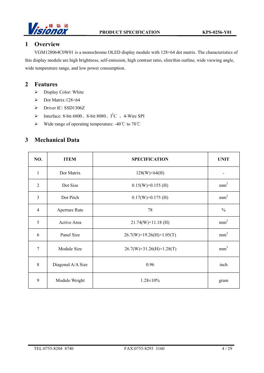
3 Mechanical Data
NO.
ITEM
1
2
3
4
5
6
7
8
9
Dot Matrix
Dot Size
Dot Pitch
Aperture Rate
Active Area
Panel Size
Module Size
Diagonal A/A Size
Module Weight
SPECIFICATION
128(W)×64(H)
0.15(W)×0.155 (H)
0.17(W)×0.175 (H)
78
21.74(W)×11.18 (H)
26.7(W)×19.26(H)×1.05(T)
26.7(W)×31.26(H)×1.28(T)
0.96
1.28±10%
UNIT
-
mm2
mm2
%
mm2
mm3
mm3
inch
gram
TEL:0755-8204 8740 FAX:0755-8293 3160 4 / 29
�
PRODUCT SPECIFICATION KPS-0256-Y01
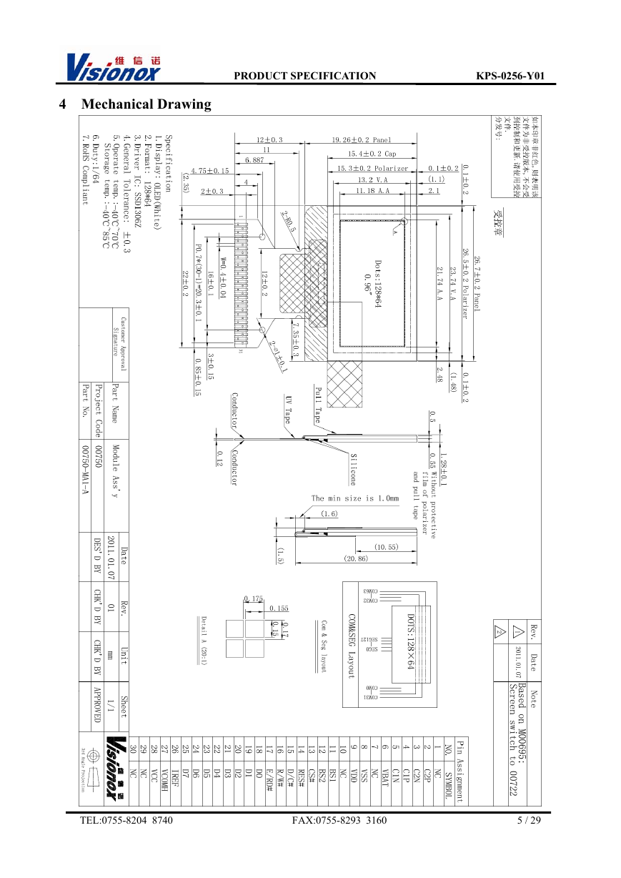
4 Mechanical Drawing
TEL:0755-8204 8740 FAX:0755-8293 3160 5 / 29
�
PRODUCT SPECIFICATION KPS-0256-Y01
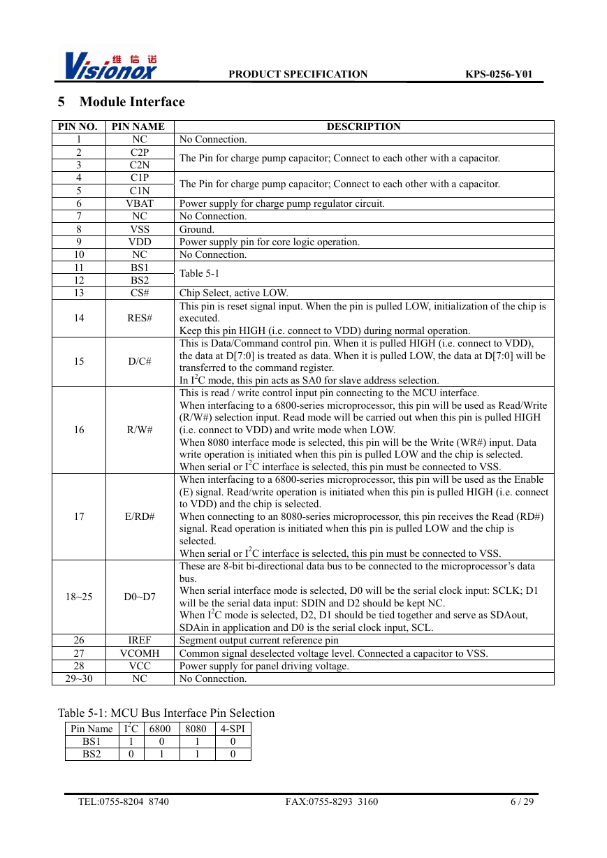
5 Module Interface
PIN NO. PIN NAME
1
2
3
4
5
6
7
8
9
10
11
12
13
NC
C2P
C2N
C1P
C1N
VBAT
NC
VSS
VDD
NC
BS1
BS2
CS#
14
15
RES#
D/C#
16
R/W#
17
E/RD#
18~25
D0~D7
26
27
28
29~30
IREF
VCOMH
VCC
NC
No Connection.
The Pin for charge pump capacitor; Connect to each other with a capacitor.
DESCRIPTION
The Pin for charge pump capacitor; Connect to each other with a capacitor.
Power supply for charge pump regulator circuit.
No Connection.
Ground.
Power supply pin for core logic operation.
No Connection.
Table 5-1
Chip Select, active LOW.
This pin is reset signal input. When the pin is pulled LOW, initialization of the chip is
executed.
Keep this pin HIGH (i.e. connect to VDD) during normal operation.
This is Data/Command control pin. When it is pulled HIGH (i.e. connect to VDD),
the data at D[7:0] is treated as data. When it is pulled LOW, the data at D[7:0] will be
transferred to the command register.
In I2C mode, this pin acts as SA0 for slave address selection.
This is read / write control input pin connecting to the MCU interface.
When interfacing to a 6800-series microprocessor, this pin will be used as Read/Write
(R/W#) selection input. Read mode will be carried out when this pin is pulled HIGH
(i.e. connect to VDD) and write mode when LOW.
When 8080 interface mode is selected, this pin will be the Write (WR#) input. Data
write operation is initiated when this pin is pulled LOW and the chip is selected.
When serial or I2C interface is selected, this pin must be connected to VSS.
When interfacing to a 6800-series microprocessor, this pin will be used as the Enable
(E) signal. Read/write operation is initiated when this pin is pulled HIGH (i.e. connect
to VDD) and the chip is selected.
When connecting to an 8080-series microprocessor, this pin receives the Read (RD#)
signal. Read operation is initiated when this pin is pulled LOW and the chip is
selected.
When serial or I2C interface is selected, this pin must be connected to VSS.
These are 8-bit bi-directional data bus to be connected to the microprocessor’s data
bus.
When serial interface mode is selected, D0 will be the serial clock input: SCLK; D1
will be the serial data input: SDIN and D2 should be kept NC.
When I2C mode is selected, D2, D1 should be tied together and serve as SDAout,
SDAin in application and D0 is the serial clock input, SCL.
Segment output current reference pin
Common signal deselected voltage level. Connected a capacitor to VSS.
Power supply for panel driving voltage.
No Connection.
Table 5-1: MCU Bus Interface Pin Selection
Pin Name
BS1
BS2
I2C 6800
1
0
1
0
8080
1
1
4-SPI
0
0
TEL:0755-8204 8740 FAX:0755-8293 3160 6 / 29
�
PRODUCT SPECIFICATION KPS-0256-Y01
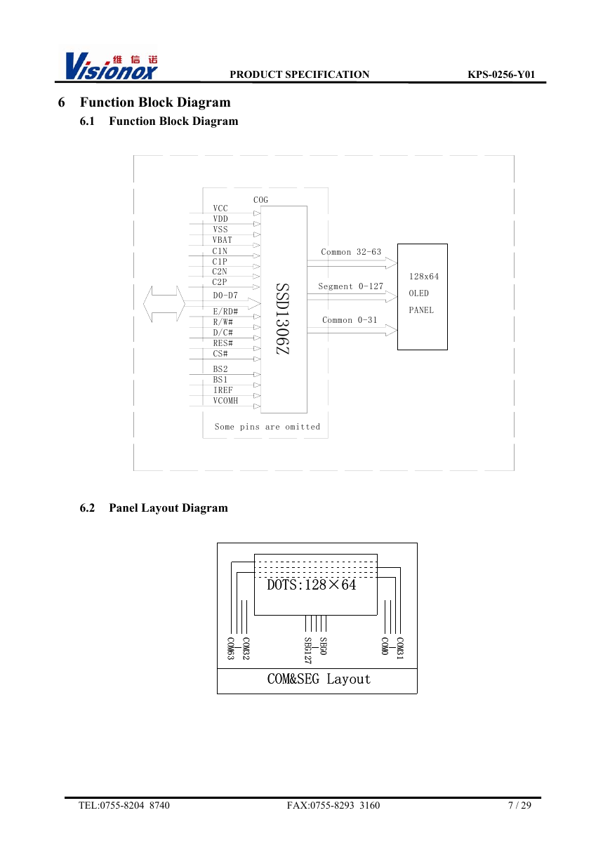
6 Function Block Diagram
6.1 Function Block Diagram
COG
S
S
D
1
3
0
6
Z
VCC
VDD
VSS
VBAT
C1N
C1P
C2N
C2P
D0-D7
E/RD#
R/W#
D/C#
RES#
CS#
BS2
BS1
IREF
VCOMH
Common 32-63
Segment 0-127
Common 0-31
128x64
OLED
PANEL
Some pins are omitted
6.2 Panel Layout Diagram
DOTS:128×64
DOTS:128×64
C
C
O
O
M
M
6
6
3
3
C
C
O
O
M
M
3
3
2
2
S
S
E
E
G
G
0
0
S
S
E
E
G
G
1
1
2
2
7
7
C
C
O
O
M
M
0
0
C
C
O
O
M
M
3
3
1
1
COM&SEG Layout
COM&SEG Layout
TEL:0755-8204 8740 FAX:0755-8293 3160 7 / 29
�
PRODUCT SPECIFICATION KPS-0256-Y01
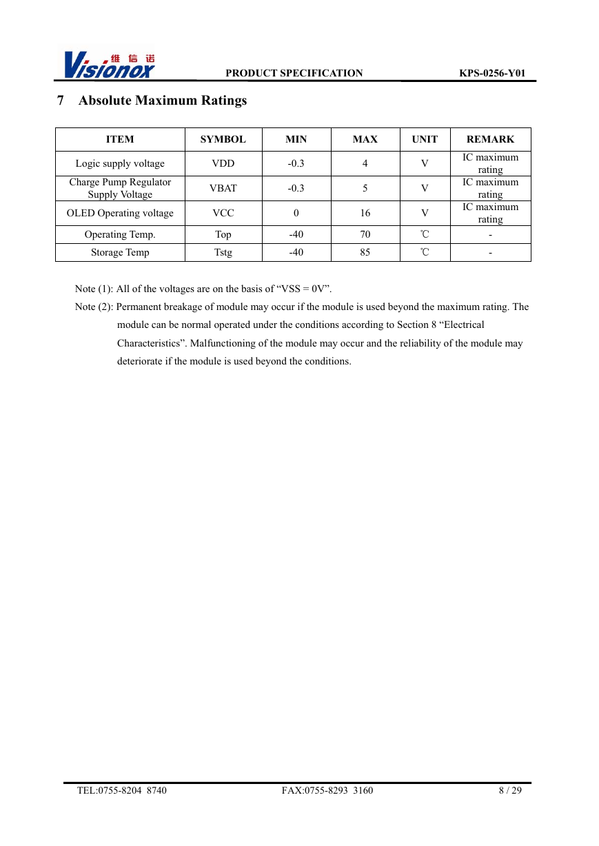
7 Absolute Maximum Ratings
ITEM
SYMBOL
MIN
MAX
UNIT
Logic supply voltage
Charge Pump Regulator
Supply Voltage
OLED Operating voltage
Operating Temp.
Storage Temp
VDD
VBAT
VCC
Top
Tstg
-0.3
-0.3
0
-40
-40
4
5
16
70
85
V
V
V
℃
℃
REMARK
IC maximum
IC maximum
rating
rating
IC maximum
rating
-
-
Note (1): All of the voltages are on the basis of “VSS = 0V”.
Note (2): Permanent breakage of module may occur if the module is used beyond the maximum rating. The
module can be normal operated under the conditions according to Section 8 “Electrical
Characteristics”. Malfunctioning of the module may occur and the reliability of the module may
deteriorate if the module is used beyond the conditions.
TEL:0755-8204 8740 FAX:0755-8293 3160 8 / 29
�
