SAMSUNG CONFIDENTIAL
Rev. 1.11, Aug. 2013
K9F1G08U0E
1Gb E-die NAND Flash
Single-Level-Cell (1bit/cell)
datasheet
SAMSUNG ELECTRONICS RESERVES THE RIGHT TO CHANGE PRODUCTS, INFORMATION AND
SPECIFICATIONS WITHOUT NOTICE.
Products and specifications discussed herein are for reference purposes only. All information discussed
herein is provided on an "AS IS" basis, without warranties of any kind.
This document and all information discussed herein remain the sole and exclusive property of Samsung
Electronics. No license of any patent, copyright, mask work, trademark or any other intellectual property
right is granted by one party to the other party under this document, by implication, estoppel or other-
wise.
Samsung products are not intended for use in life support, critical care, medical, safety equipment, or
similar applications where product failure could result in loss of life or personal or physical harm, or any
military or defense application, or any governmental procurement to which special terms or provisions
may apply.
For updates or additional information about Samsung products, contact your nearest Samsung office.
All brand names, trademarks and registered trademarks belong to their respective owners.
ⓒ 2013 Samsung Electronics Co., Ltd. All rights reserved.
- 1 -
�
datasheet
SAMSUNG CONFIDENTIAL
Rev. 1.11
FLASH MEMORY
K9F1G08U0E
Revision History
Revision No.
History
Draft Date
Remark
Edited by Reviewed by
0.0
0.01
0.1
1.0
1.1
1. Initial issue
1. Typo corrected.
Chapter 4.3 Input Data Latch Cycle
Chapter 4.11 Copy-Back Program Operation with Random Data Input
revised.
1. read ID revised
1. Corrected errata
1.11
1. Industrial product feature added
Dec. 17, 2012
Feb.02, 2013
Feb.22, 2013
Target
Target
Target
Jul.03, 2013
Aug.06, 2013
Aug.07, 2013
Final
Final
Final
H.K.Kim
H.K.Kim
H.K.Kim
S.M.Lee
S.M.Lee
S.M.Lee
H.H.Shin
H.H.Shin
H.H.Shin
H.H.Shin
H.H.Shin
H.H.Shin
- 2 -
�
K9F1G08U0E
datasheet
SAMSUNG CONFIDENTIAL
Rev. 1.11
FLASH MEMORY
Table Of Contents
1.0 INTRODUCTION ........................................................................................................................................................4
1.1 General Description................................................................................................................................................. 4
1.2 Features ................................................................................................................................................................. 4
1.3 General Description................................................................................................................................................. 4
1.4Pin Configuration (TSOP1)....................................................................................................................................... 5
1.4.1 Package Dimensions ........................................................................................................................................ 5
1.5 Pin Configuration (FBGA)........................................................................................................................................ 6
1.5.1 Package Dimensions ........................................................................................................................................ 7
1.6 Pin Description ........................................................................................................................................................ 8
2.0 PRODUCT INTRODUCTION......................................................................................................................................10
2.1 Absolute Maximum Ratings..................................................................................................................................... 11
2.2 Recommended Operating Conditions ..................................................................................................................... 11
2.3 DC And Operating Characteristics(Recommended operating conditions otherwise noted.) ................................... 11
2.4 Valid Block.............................................................................................................................................................. 12
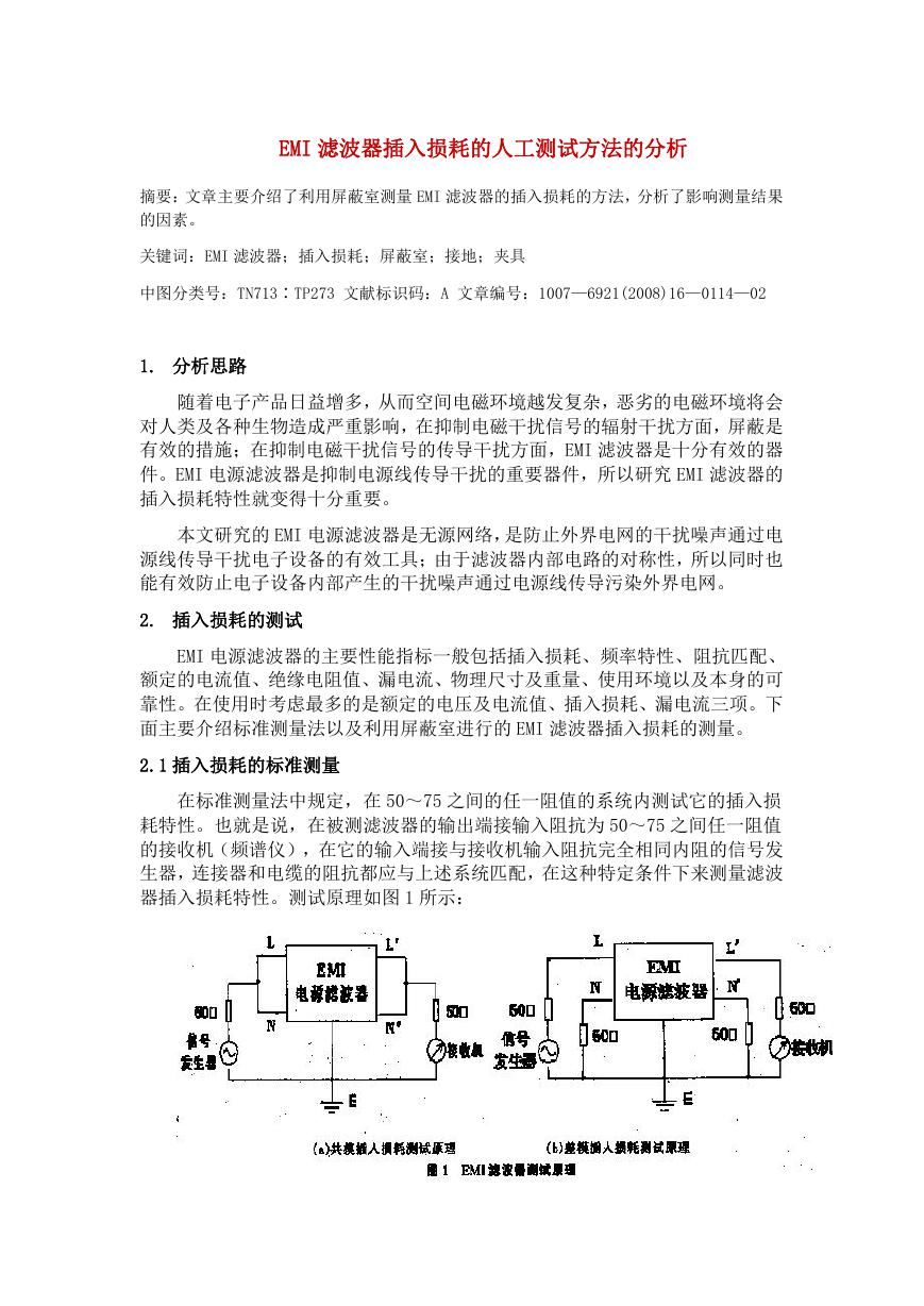
2.5 AC Test Condition ................................................................................................................................................... 12
2.6 Capacitance(TA=25°C, VCC=3.3V, f=1.0MHz)....................................................................................................... 12
2.7 Mode Selection........................................................................................................................................................ 12
2.8 Program / Erase Characteristics.............................................................................................................................. 13
2.9 AC Timing Characteristics for Command / Address / Data Input ............................................................................ 13
2.10 AC Characteristics for Operation........................................................................................................................... 14
3.0 NAND FLASH TECHNICAL NOTES ..........................................................................................................................15
3.1 Initial Invalid Block(s)............................................................................................................................................... 15
3.2 Identifying Initial Invalid Block(s) ............................................................................................................................. 15
3.3 Error in Write or Read Operation............................................................................................................................. 16
3.4 Addressing for Program Operation.......................................................................................................................... 18
4.0 SYSTEM INTERFACE USING CE DON’T-CARE. .....................................................................................................19
4.1 Command Latch Cycle ............................................................................................................................................ 20
4.2 Address Latch Cycle................................................................................................................................................ 20
4.3 Input Data Latch Cycle ............................................................................................................................................ 21
4.4 Status Read Cycle................................................................................................................................................... 22
4.5 Read Operation ....................................................................................................................................................... 23
4.6 Read Operation(Intercepted by CE) ........................................................................................................................ 23
4.7 Random Data Output In a Page ............................................................................................................................. 24
4.8 Page Program Operation......................................................................................................................................... 25
4.9 Page Program Operation with Random Data Input ................................................................................................. 26
4.10 Copy-Back Program Operation ............................................................................................................................. 27
4.11 Copy-Back Program Operation with Random Data Input...................................................................................... 28
4.12 Block Erase Operation........................................................................................................................................... 29
4.13 Read ID Operation................................................................................................................................................. 29
5.0 DEVICE OPERATION ................................................................................................................................................32
5.1 Page Read............................................................................................................................................................... 32
5.2 Page Program ......................................................................................................................................................... 33
5.3 Copy-Back Program ................................................................................................................................................ 34
5.4 Block Erase ............................................................................................................................................................. 35
5.5 Read Status............................................................................................................................................................. 35
5.6 Read ID ................................................................................................................................................................... 36
5.7 Reset ....................................................................................................................................................................... 36
5.8 Ready/busy.............................................................................................................................................................. 37
6.0 DEVICE OPERATION ................................................................................................................................................38
- 3 -
�
datasheet
SAMSUNG CONFIDENTIAL
Rev. 1.11
FLASH MEMORY
K9F1G08U0E
1.0 INTRODUCTION
1.1 General Description
Part Number
K9F1G08U0E-S
K9F1G08U0E-B
Vcc Range
2.7V ~ 3.6V
2.7V ~ 3.6V
Organization
x8
x8
PKG Type
TSOP1
63FBGA
1.2 Features
Voltage Supply
- 3.3V Device(K9F1G08U0E) : 2.7V ~ 3.6V
Organization
- Memory Cell Array : (128M + 4M) x 8bit
- Data Register : (2K + 64) x 8bit
Automatic Program and Erase
- Page Program : (2K + 64)Byte
- Block Erase : (128K + 4K)Byte
Page Read Operation
- Page Size : (2K + 64)Byte
- Random Read : 40s(Max.)
- Serial Access : 25ns(Min.)
Fast Write Cycle Time
- Page Program time : 400s(Typ.)
- Block Erase Time : 4.5ms(Typ.)
Command/Address/Data Multiplexed I/O Port
Hardware Data Protection
- Program/Erase Lockout During Power Transitions
Reliable CMOS Floating-Gate Technology
-Endurance & Data Retention : Refor to the gualification report
-ECC regnirement : 1 bit / 528bytes
Command Driven Operation
Unique ID for Copyright Protection
Package :
- K9F1G08U0E-SCB0/SIB0 : Pb-FREE PACKAGE
48 - Pin TSOP I (12 x 20 / 0.5 mm pitch)
- K9F1G08U0E-BCB0/BIB0 : Pb-FREE PACKAGE
63 FBGA (9 x 11 / 0.8 mm pitch)
1.3 General Description
Offered in 128Mx8bit, the K9F1G08U0E is a 1G-bit NAND Flash Memory with spare 32M-bit. Its NAND cell provides the most cost-effective solution for
the solid state application market. A program operation can be performed in typical 400s on the (2K+64)Byte page and an erase operation can be per-
formed in typical 4.5ms on a (128K+4K)Byte block. Data in the data register can be read out at 25ns cycle time per Byte. The I/O pins serve as the ports
for address and data input/output as well as command input. The on-chip write controller automates all program and erase functions including pulse rep-
etition, where required, and internal verification and margining of data. Even the write-intensive systems can take advantage of the K9F1G08U0Es
extended reliability by providing ECC(Error Correcting Code) with real time mapping-out algorithm. The K9F1G08U0E is an optimum solution for large
nonvolatile storage applications such as solid state file storage and other portable app.lications requiring non-volatility.
- 4 -
�
K9F1G08U0E
1.4Pin Configuration (TSOP1)
datasheet
K9F1G08U0E-SCB0/SIB0
SAMSUNG CONFIDENTIAL
Rev. 1.11
FLASH MEMORY
N.C
N.C
N.C
N.C
N.C
N.C
R/B
RE
CE
N.C
N.C
Vcc
Vss
N.C
N.C
CLE
ALE
WE
WP
N.C
N.C
N.C
N.C
N.C
1
2
3
4
5
6
7
8
9
10
11
12
13
14
15
16
17
18
19
20
21
22
23
24
48-pin TSOP1
Standard Type
12mm x 20mm
48
47
46
45
44
43
42
41
40
39
38
37
36
35
34
33
32
31
30
29
28
27
26
25
N.C
N.C
N.C
N.C
I/O7
I/O6
I/O5
I/O4
N.C
N.C
N.C
Vcc
Vss
N.C
N.C
N.C
I/O3
I/O2
I/O1
I/O0
N.C
N.C
N.C
N.C
1.4.1 Package Dimensions
48-PIN LEAD FREE PLASTIC THIN SMALL OUT-LINE PACKAGE TYPE(I)
48 - TSOP1 - 1220AF
Unit :mm/Inch
20.000.20
0.7870.008
#1
.
7
0
0
+
3
0
0
-
.
0
2
.
0
.
7
0
0
+
3
0
0
-
.
6
1
.
0
.
.
3
0
0
0
+
1
0
0
0
-
8
0
0
.
0
0
5
.
0
7
9
1
0
.
0
#24
P
Y
T
5
2
.
0
1
0
18.400.10
0.7240.004
0
.
0
0~8
0.45~0.75
0.018~0.030
X
A
M
0
1
.
0
4
0
0
.
0
#48
#25
5
7
0
.
0
+
5
3
0
.
0
5
2
1
.
0
3
0
0
.
0
+
1
0
0
.
0
-
5
0
0
.
0
)
5
2
.
0
0
1
0
.
0
(
X
A
M
0
4
.
2
1
8
8
4
.
0
0
0
.
2
1
2
7
4
.
0
0.05 MIN
0.002
1.000.05
0.0390.002
1.20 MAX
0.047
(
0.50
0.020
)
- 5 -
�
SAMSUNG CONFIDENTIAL
Rev. 1.11
FLASH MEMORY
K9F1G08U0E
1.5 Pin Configuration (FBGA)
datasheet
K9F1G08U0E-BCB0/BIB0
Top View
4
6
5
1
2
3
7
8
9
10
N.C N.C
N.C
N.C N.C
N.C
N.C
/WP
ALE
Vss
/CE
/WE
R/B
NC
/RE CLE
NC
NC
NC
NC
NC
NC
NC
NC
NC
NC
NC
NC
NC
NC
NC
NC
NC
NC
NC
NC
NC
NC I/O0
NC
NC
NC Vcc
NC
I/O1
NC Vcc
I/O5 I/O7
Vss
I/O2
I/O3
I/O4
I/O6
Vss
N.C N.C
N.C
N.C
N.C N.C
N.C
N.C
A
B
C
D
E
F
G
H
J
K
L
M
- 6 -
�
datasheet
SAMSUNG CONFIDENTIAL
Rev. 1.11
FLASH MEMORY
K9F1G08U0E
1.5.1 Package Dimensions
63-Ball FBGA (measured in millimeters)
9.000.10
#A1
X
A
M
0
1
.
0
0
1
.
0
0
0
.
1
1
(Datum B)
A
B
C
D
E
F
G
H
J
K
L
M
9.000.10
0.80 x 9= 7.20
3.60
0.80
8
7
6
0.40
4
5
10
9
3
2
1
A
#A1 INDEX MARK
B
0
4
.
4
0
8
.
8
=
1
1
x
0
8
0
.
0
1
.
0
0
0
.
1
1
0
4
.
0
0
8
.
0
0.320.05
0.900.10
63-0.450.05
0.2 M A B
(Datum A)
TOP VIEW
SIDE VIEW
BOTTOM VIEW
- 7 -
�
K9F1G08U0E
1.6 Pin Description
datasheet
SAMSUNG CONFIDENTIAL
Rev. 1.11
FLASH MEMORY
Pin Name
I/O0 ~ I/O7
CLE
ALE
CE
RE
WE
WP
R/B
Vcc
Vss
N.C
Pin Function
DATA INPUTS/OUTPUTS
The I/O pins are used to input command, address and data, and to output data during read operations. The I/O pins float to
high-z when the chip is deselected or when the outputs are disabled.
COMMAND LATCH ENABLE
The CLE input controls the activating path for commands sent to the command register. When active high, commands are
latched into the command register through the I/O ports on the rising edge of the WE signal.
ADDRESS LATCH ENABLE
The ALE input controls the activating path for address to the internal address registers. Addresses are latched on the rising
edge of WE with ALE high.
CHIP ENABLE
The CE input is the device selection control. When the device is in the Busy state, CE high is ignored, and the device does
not return to standby mode in program or erase operation.
READ ENABLE
The RE input is the serial data-out control, and when active drives the data onto the I/O bus. Data is valid tREA after the fall-
ing edge of RE which also increments the internal column address counter by one.
WRITE ENABLE
The WE input controls writes to the I/O port. Commands, address and data are latched on the rising edge of the WE pulse.
WRITE PROTECT
The WP pin provides inadvertent program/erase protection during power transitions. The internal high voltage generator is
reset when the WP pin is active low.
READY/BUSY OUTPUT
The R/B output indicates the status of the device operation. When low, it indicates that a program, erase or random read
operation is in process and returns to high state upon completion. It is an open drain output and does not float to high-z con-
dition when the chip is deselected or when outputs are disabled.
POWER
VCC is the power supply for device.
GROUND
NO CONNECTION
NOTE :
Connect all VCC and VSS pins of each device to common power supply outputs.
- 8 -
�

.pdf-第1页.jpg")
.pdf-第2页.jpg")
.pdf-第3页.jpg")
.pdf-第4页.jpg")
.pdf-第5页.jpg")
.pdf-第6页.jpg")
.pdf-第7页.jpg")
.pdf-第8页.jpg")
 V2版本原理图(Capacitive-Fingerprint-Reader-Schematic_V2).pdf
 摄像头工作原理.doc
 VL53L0X简要说明(En.FLVL53L00216).pdf
 原理图(DVK720-Schematic).pdf
 原理图(Pico-Clock-Green-Schdoc).pdf
 原理图(RS485-CAN-HAT-B-schematic).pdf
 File:SIM7500_SIM7600_SIM7800 Series_SSL_Application Note_V2.00.pdf
 ADS1263(Ads1262).pdf
 原理图(Open429Z-D-Schematic).pdf
 用户手册(Capacitive_Fingerprint_Reader_User_Manual_CN).pdf
 CY7C68013A(英文版)(CY7C68013A).pdf
 TechnicalReference_Dem.pdf